LP5551SQX/NOPB National Semiconductor, LP5551SQX/NOPB Datasheet
LP5551SQX/NOPB
Specifications of LP5551SQX/NOPB


Related parts for LP5551SQX/NOPB


LP5551SQX/NOPB Summary of contents
Page 1
... P- and N-well biasing for threshold scal- ing. System Diagram © 2007 National Semiconductor Corporation Features ■ 2 300 mA buck regulators operate 180 degrees out of phase for reduced EMI ■ ...
Page 2
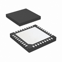
Connection Diagrams and Package Mark Information 36 - Pin LLP Package Mark Note: The actual physical placement of the package marking will vary from part to part. www.national.com NS Package Number SQA36A FIGURE 2. LP5551 Pinout 20172146 FIGURE 3. Top ...
Page 3
Typical Application Pin Descriptions Pin # Name I/O Type 0 DAP GP3 GP2 GP1 GP0 PWROK O D FIGURE 4. Typical Application Circuit Description Connect ...
Page 4
Pin # Name I/O Type 6 RESETN SPWI I SCLK LDO2 LDO4 LDO1 LDO3 ...
Page 5
... Absolute Maximum Ratings If Military/Aerospace specified devices are required, please contact the National Semiconductor Sales Office/ Distributors for availability and specifications. VDD_A, VDD_D, PVDD1, and PVDD2 LDO1, LDO2, LDO3, LDO4, -0.3 to VDD_A + 0.3V VNWELL to GND, VPwell, ENABLE, RESETN, FB1, FB2, SW_AVS, SW_DVS,GP0, GP1, GP2, and GP3 SPWI, SCLK, PWROK -0 ...
Page 6
Symbol Parameter ΔV Line Regulation OUT Load Regulation Line Transient Regulation Load Transient Regulation eN Output Noise Voltage PSRR Power Supply Ripple Rejection Ratio C Output Capacitance OUT Output Capacitor ESR t Start-Up Time from Shut-down C START-UP LDO2 (I/O ...
Page 7
Symbol Parameter C Output Capacitance OUT Output Capacitor ESR t Start-Up Time from Shut-down C START-UP LDO3 (Memory Retention Voltage) Characteristics V RESETN, ENABLE = 3.6V. Typical values and limits appearing in normal type apply for TJ = 25°C. Limits ...
Page 8
Symbol Parameter ΔV Line Regulation OUT Load Regulation Line Transient Regulation Load Transient Regulation eN Output Noise Voltage PSRR Power Supply Ripple Rejection Ratio C Output Capacitance OUT Output Capacitor ESR t Start-Up Time from Shut-down C START-UP AVS/DVS Switcher ...
Page 9
N-Well Bias Characteristics values and limits appearing in normal type apply for TJ = 25°C. Limits appearing in boldface type apply over the entire junction temperature range for operation, -40 to +125°C. (Notes Symbol Parameter V Output ...
Page 10
Symbol Parameter I Output Sinking Capability SINK I Output Source Capability SOURCE C Output Capacitance of Load LOAD Logic and Control Inputs and limits appearing in normal type apply for TJ = 25°C. Limits appearing in boldface type apply over ...
Page 11
... Note 4: For detailed soldering specifications and information, please refer to National Semiconductor Application Note 1187: Leadless Leadframe Package (LLP) (AN-1187). Note 5: In applications where high power dissipation and/or poor package thermal resistance is present, the maximum ambient temperature may have to be derated. Maximum ambient temperature (TA-MAX) is dependent on the maximum operating junction temperature (TJ-MAX-OP = 125°C), the maximum power dissipation of the device in the application (PD-MAX), and the junction-to ambient thermal resistance of the part/package in the application (θ ...
Page 12
Simplified Functional Diagram www.national.com FIGURE 5. Simplified Functional Diagram 12 20172132 ...
Page 13
Typical Performance Characteristics I vs Sleep, no load on LDO3 Start-up Sequence All Outputs at Maximum Rated Load Line Transient Response O2/4 Unless otherwise stated: V 20172104 Line Transient Response 20172106 Load Transient ...
Page 14
Load Transient Resoponse V O1 LDO2/4 PSRR Switching Frequency vs. V www.national.com 20172155 20172158 Load Transient Response IN AVS/DVS Switcher, Automatic PWM/PFM Transition 20172110 14 LDO1 PSRR 20172157 LDO3 PSRR 20172159 20172113 ...
Page 15
Load Trainsiet Response AVS/DVS Switcher, PWM only 20172114 V Transient Response OUT Min to Max Transient 20172116 Switch Current Limit vs 20172118 Load Transient Response AVS/DVS Switcher, PFM only V Transient Response OUT Max to Min Transient Efficiency ...
Page 16
Switching Waveforms PWM LP5551 PWI Register Map The PWI standard supports sixteen 8-bit registers on the PWI slave. The table below summarizes these registers and shows default register bit values after reset. The following sub-sections provide additional detail on the ...
Page 17
Bit Field Name 7 Sign 6:0 Voltage R1 - Unused Register Address 0x1 Type R/W Reset Default 8h’00 Bit Field Name 7:0 Unused R2 – VO3 Voltage Register (Memory Retention Voltage) Address 0x2 Type R/W Reset Default 8h’60 Bit Field ...
Page 18
R3 - Status Register Address 0x3 Type Read Only Reset Default 8h’0F Bit Field Name 7 Reserved 6 Reserved 5 User Bit 4 User Bit 3 Fixed Memory OK 0 Core PWI ...
Page 19
Bit Field Name 7 Sign 6:2 Voltage 0:1 Unused R7 – VO2 Voltage Register (I/O Voltage) Address 0x7 Type R/W Reset Default 8h’78 Bit Field Name 7 Sign 6:3 Voltage 2:0 Unused R8 – VO1 Voltage Register (PLL/Fixed Voltage) Address ...
Page 20
Bit Field Name 7 Sign 6:3 Voltage 2:0 Unused R9– PFM/PWM Force Register Address 0x9 Type R/W Reset Default 8h’00 Bit Field Name Description or Comment 7:4 Unused These bits are fixed to ‘0’. Reading these bits will result in ...
Page 21
Bit Field Name 7 Sign 6:0 Voltage R11 – Enable Control Register Address 0xB Type R/W Reset Default 8h’3F Bit Field Name 7:6 Unused 5 R10 Enable (DVS Switcher Enable (LDO Enable (LDO 1) 2 ...
Page 22
Bit Field Name 7 Sign 6:3 Voltage 2:0 Unused R13 – GPO Control Address 0xD Type R/W Reset Default 8h’00 Bit Field Name 7:6 Unused 5:4 P-Well Sink Current Control 3 GPO_3 control 2 GPO_2 control 1 GPO_1 control 0 ...
Page 23
Bit Field Name 7:0 Unused Description or Comment Write transactions to this register are ignored. Read transactions will return a “No Response Frame.” response frame contains all zeros (see PWI 1.0 specification) frame. 23 www.national.com ...
Page 24
R15 – Manufacturer Register Adress 0xF Bit Field Name 7:0 Reserved www.national.com Type R/W Reset Default 8h'00 Description or Comment Do not write to this register 24 ...
Page 25
Operation Description DEVICE INFORMATION The LP5551 is a PowerWise Interface (PWI) compliant power management unit (PMU) for application or baseband proces- sors in mobile phones or other portable equipment. It oper- ates cooperatively with processors Semiconductor’s Advanced Power Controller (APC) ...
Page 26
VOLTAGE SCALING The LP5551 is designed to be used in a voltage scaling sys- tem to lower the power dissipation of baseband or application processors in mobile phones or other portable equipment. By scaling supply voltage with the clock frequency ...
Page 27
Application Information PWM/PFM FORCE REGISTER (R9) By default, the LP5551 automatically transitions between PFM and PWM to optimize efficiency. The PWM/PFM force register (R9) provides the option to override the automatic transition and force PFM or PWM operation (see R9 ...
Page 28
Ceramic capacitors are predominately used in portable systems and have very low ESR and remain capac- itive up to high frequencies. The switcher peak - to - peak output voltage ripple in steady state can be calculated as: ...
Page 29
BOARD LAYOUT CONSIDERATIONS FIGURE 9. Board Layout Design Recommendations for the LP5551 29 20172161 www.national.com ...
Page 30
Physical Dimensions www.national.com inches (millimeters) unless otherwise noted 36-Lead LLP Package NS Package Number SQA36A 30 ...
Page 31
Notes 31 www.national.com ...
Page 32
... National Semiconductor and the National Semiconductor logo are registered trademarks of National Semiconductor Corporation. All other brand or product names may be trademarks or registered trademarks of their respective holders. ...