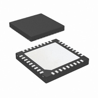
LP5551SQX/NOPB National Semiconductor, LP5551SQX/NOPB Datasheet - Page 26

LP5551SQX/NOPB
Manufacturer Part Number
LP5551SQX/NOPB
Description
IC ENERGY MGMNT SYSTEM 36-LLP
Manufacturer
National Semiconductor
Series
PowerWise®r
Datasheet
1.LP5551SQXNOPB.pdf
(32 pages)
Specifications of LP5551SQX/NOPB
Applications
Handheld/Mobile Devices
Current - Supply
431µA
Voltage - Supply
2.7 V ~ 5.5 V
Operating Temperature
-40°C ~ 85°C
Mounting Type
Surface Mount
Package / Case
36-LLP
For Use With
LP5551SQEV - BOARD EVALUATION LP5551SQ
Lead Free Status / RoHS Status
Lead free / RoHS Compliant
Other names
LP5551SQX
www.national.com
VOLTAGE SCALING
The LP5551 is designed to be used in a voltage scaling sys-
tem to lower the power dissipation of baseband or application
processors in mobile phones or other portable equipment. By
scaling supply voltage with the clock frequency of a proces-
sor, dramatic power savings can be achieved. Two types of
voltage scaling are supported, dynamic voltage scaling (DVS)
and adaptive voltage scaling (AVS). DVS systems switch be-
tween pre-characterized voltages which are paired to clock
frequencies used for frequency scaling in the processor. AVS
systems track the processor performance and optimize the
supply voltage to the required performance. AVS is a closed
loop system that provides process and temperature compen-
sation such that for any given processor, temperature, or
clock frequency, the minimum supply voltage is delivered.
DIGITALLY CONTROLLED VOLTAGE SCALING
The LP5551 delivers fast, controlled voltage scaling tran-
sients with the help of a digital state machine. The state
machine automatically optimizes the control loop in the
LP5551 switching regulator to provide large signal transients
with minimal over- and undershoot. This is an important char-
acteristic for voltage scaling systems that rely on minimal
over- and undershoot to set voltages as low as possible and
save energy.
LARGE SIGNAL TRANSIENT RESPONSE
The switching converter in the LP5551 is designed to work in
a voltage scaling system. This requires that the converter has
a well controlled large signal transient response. Specifically,
the under- and over-shoots have to be minimal or zero while
maintaining settling times less than 100 usec. Typical re-
sponse plots are shown in the Typical Performance section.
PowerWise™ INTERFACE
To support DVS and AVS, the LP5551 is programmable via
the low power, 2 wire PowerWise Interface (PWI). This serial
interface controls the various voltages and states of all the
regulators in the LP5551. In particular, the switching regulator
voltage can be controlled between 0.6V and 1.2V in 128 steps
(linear scaling). This high resolution voltage control affords
accurate temperature and process compensation in AVS.
The LDO voltages can also be set, however they are not in-
tended to be dynamic in operation. The LP5551 supports the
full command set as described in PWI 1.0 specification:
•
•
•
•
•
•
•
•
•
PWM/PFM OPERATION
The switching converter in the LP5551 has two modes of op-
eration: pulse width modulation (PWM) and pulse frequency
Core Voltage Adjust
Reset
Sleep
Shutdown
Wakeup
Register Read
Register Write
Authenticate
Synchronize
26
modulation (PFM). In PWM the converter switches at 1MHz.
Each period can be split into two cycles. During the first cycle,
the high-side switch is on and the low-side switch is off, there-
fore the inductor current is rising. In the second cycle, the
high-side switch is off and the low-side switch is on causing
the inductor current to decrease. The output ripple voltage is
lowest in PWM mode Figure 7. As the load current decreases,
the converter efficiency becomes worse due to the increased
percentage of overhead current needed to operate in PWM
mode. The LP5551 can operate in PFM mode to increase ef-
ficiency at low loads.
By default, the part will automatically transition into PFM
mode when either of two conditions occurs for a duration of
32 or more clock cycles:
level:
During PFM operation, the converter positions the output volt-
age slightly higher than the nominal output voltage during
PWM operation, allowing additional headroom for voltage
drop during a load transient from light to heavy load. The PFM
comparators sense the output voltage via the feedback pin
and control the switching of the output FETs such that the
output voltage ramps between 0.8% and 1.6% (typ) above the
nominal PWM output voltage. If the output voltage is below
the ‘high’ PFM comparator threshold, the PMOS power switch
is turned on. It remains on until the output voltage exceeds
the ‘high’ PFM threshold or the peak current exceeds the
I
is:
FIGURE 7. Operation in PFM Mode and Transfer to PWM
PFM
A.
B.
level set for PFM mode. The peak current in PFM mode
The inductor valley current goes below 0 A
The peak PMOS switch current drops below the I
Mode
20172103
MODE


