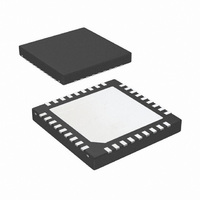
LP5551SQX/NOPB National Semiconductor, LP5551SQX/NOPB Datasheet - Page 11

LP5551SQX/NOPB
Manufacturer Part Number
LP5551SQX/NOPB
Description
IC ENERGY MGMNT SYSTEM 36-LLP
Manufacturer
National Semiconductor
Series
PowerWise®r
Datasheet
1.LP5551SQXNOPB.pdf
(32 pages)
Specifications of LP5551SQX/NOPB
Applications
Handheld/Mobile Devices
Current - Supply
431µA
Voltage - Supply
2.7 V ~ 5.5 V
Operating Temperature
-40°C ~ 85°C
Mounting Type
Surface Mount
Package / Case
36-LLP
For Use With
LP5551SQEV - BOARD EVALUATION LP5551SQ
Lead Free Status / RoHS Status
Lead free / RoHS Compliant
Other names
LP5551SQX
Note 4: For detailed soldering specifications and information, please refer to National Semiconductor Application Note 1187: Leadless Leadframe Package (LLP)
(AN-1187).
Note 5: In applications where high power dissipation and/or poor package thermal resistance is present, the maximum ambient temperature may have to be
derated. Maximum ambient temperature (TA-MAX) is dependent on the maximum operating junction temperature (TJ-MAX-OP = 125°C), the maximum power
dissipation of the device in the application (PD-MAX), and the junction-to ambient thermal resistance of the part/package in the application (θ
), as given by the
JA
following equation: TA-MAX = TJ-MAX-OP – (θJA × PD-MAX).
Note 6: Junction-to-ambient thermal resistance (θJA) is taken from a thermal modeling result, performed under the conditions and guidelines set forth in the
JEDEC standard JESD51-7. The test board is a 4-layer FR-4 board measuring 102mm x 76mm x 1.6mm with a 2x1 array of thermal vias. The ground plane on
the board is 50mm x 50mm. Thickness of copper layers are 36µm/18µm/18µm/36µm (1.5oz/1oz/1oz/1.5oz). Ambient temperature in simulation is 22°C, still air.
Power dissipation is 1W.
Junction-to-ambient thermal resistance is highly application and board-layout dependent. In applications where high maximum power dissipation exists, special
care must be paid to thermal dissipation issues in board design.
The value of θ
of this product can vary significantly, depending on PCB material, layout, and environmental conditions. In applications where high maximum
JA
power dissipation exists (high VIN, high IOUT), special care must be paid to thermal dissipation issues. For more information on these topics, please refer to
Application Note 1187: Leadless Leadframe Package (LLP) and the Power Efficiency and Power Dissipation section of this datasheet.
Note 7: All limits are guaranteed by design, test and/or statistical analysis. All electrical characteristics having room-temperature limits are tested during production
with TJ = 25C. All hot and cold limits are guaranteed by correlating the electrical characteristics to process and temperature variations and applying statistical
process control.
Note 8: Capacitors: Low-ESR Surface-Mount Ceramic Capacitors are (MLCCs) used in setting electrical characteristics
Note 9: Guaranteed by design.
Note 10: Dropout voltage is the input-to-output voltage difference at which the output voltage is 100mV below its nominal value. This specification does not apply
in cases it implies operation with an input voltage below the 2.7V minimum appearing under Operating Ratings. For example, this specification does not apply
for devices having 1.5V outputs because the specification would imply operation with an input voltage at or about 1.5V
Note 11: Quiescent current for LDO1, LDO2, LDO3, and LDO4 do not include shared functional blocks such as the bandgap reference.
Note 12: The output voltage is guaranteed not to drop more than 15 mV (V
< V
- 15 mV) while sinking the specified current.
OUT
OUT(NOM)
11
www.national.com


