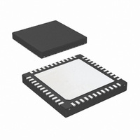
LP3913SQX-AC/NOPB National Semiconductor, LP3913SQX-AC/NOPB Datasheet - Page 11

LP3913SQX-AC/NOPB
Manufacturer Part Number
LP3913SQX-AC/NOPB
Description
IC PWR MANAGEMENT W/CHRGR 48-LLP
Manufacturer
National Semiconductor
Series
PowerWise®r
Datasheet
1.LP3913SQ-ACNOPB.pdf
(58 pages)
Specifications of LP3913SQX-AC/NOPB
Applications
Handheld/Mobile Devices
Voltage - Supply
2.5 V ~ 6 V
Operating Temperature
-40°C ~ 85°C
Mounting Type
Surface Mount
Package / Case
48-LLP
Lead Free Status / RoHS Status
Lead free / RoHS Compliant
Current - Supply
-
Other names
LP3913SQX-AC
ΔV
I
I
I
F
η
T
VIN4
V
ΔV
I
I
I
F
η
T
V
INL
DNL
V
VBATT,
RANGE 0
V
RANGE 1
OUT
PFM
Q
OUT
PFM
Q
OSC
ON
OSC
ON
OUT
REF
GP_IN
BATT,
BUCK3 Electrical Characteristics
Unless otherwise noted, VIN4 = 3.6V, C
apply for T
C. Modulation mode is PWM mode with automatic switch to PFM at light loads.
ADC Electrical Characteristics
External components:
Symbol
OUT
OUT
Symbol
Symbol
Range
J
= 25°C. Limits appearing in boldface type apply over the entire junction temperature range for operation, 0°C to +125°
Reference Voltage
Core ADC Integral Non-linearity
Core ADC Differential Non-linearity
General Purpose ADC Input Voltage
Range
Battery Max Voltage Scalar Output
Battery Min Voltage Scalar Output
Battery Max Voltage Scalar Output
Battery Min Voltage Scalar Output
Static Output Voltage Tolerance
Line Regulation
Load Regulation
Continuous Output Current
Peak Output Current Limit
Max I
Quiescent Current
Internal Oscillator Frequency
Peak Efficiency
Turn-on Time
Input Voltage
Output Voltage Programming Range
Static Output Voltage Tolerance
Line Regulation
Load Regulation
Continuous Output Current
Peak Inductor Current Limit
Max I
Quiescent Current
Internal Oscillator Frequency
Peak Efficiency
Turn-on Time
LOAD
LOAD
, PFM Mode
, PFM Mode
Parameter
Parameter
Parameter
VIN4
= 10 µF, C
BB
I
Load Regulation
I
V
100 mA < I
I
Buck2 Disabled
PWM Mode
To 95% Level (Note 9)
I
1.80V – 3.30V in 50 mV Steps
I
and Load Regulation
I
100 mA < I
V
1A Load at V
I
Buck3 Disabled
PWM Mode
To 95% Level (Note 9)
T = 25°C
T = 0°C to +125°C
V
V
VBATT = 3.5V
VBATT = 2.6V
VBATT = 4.4V
V
OUT
OUT
OUT
OUTMAX
OUT
OUT
OUT
IN3
OUT
REF
REF
REF
= 22 µF, L
= 0 mA–500 mA, Including Line
= 200 mA, Including Line and
= 10 mA
= 2.5V − V
= 0 mA
= 10 mA
= 0 mA PFM No Switching
= 3.3V
= 1.225 (Note 9)
= 1.225 (Note 9)
= 2.6V
= 500 mA
11
OUT
OUT
Conditions
Conditions
Conditions
BB
IN
< 300 mA
= 2.2 µH Typical values and limits appearing in normal type
< 500 mA
DD
= 2.7V
1.220
1.200
2.435
1.217
2.435
1.217
Min
600
850
Min
500
900
V
2.7
1.8
Min
-0.5
−3
−4
-1
REF
0.0016
0.002
1000
1.225
1.225
1.225
1.225
Typ
Typ
0.2
0.2
2.45
2.45
75
30
90
75
80
93
Typ
2
2
2·V
1150
1200
1.230
1.230
2.465
1.232
2.465
1.232
Max
Max
Max
5.7
3.3
90
0.5
3
1
1
4
1
1
1
www.national.com
REF
Units
%/mA
%/mA
Units
Units
MHz
MHz
%/V
%/V
LSB
LSB
mA
mA
mA
mA
mA
mA
ms
ms
µA
µA
%
%
%
%
V
V
V
V
V
V
V
V
V


