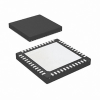
LP3913SQX-AC/NOPB National Semiconductor, LP3913SQX-AC/NOPB Datasheet - Page 9

LP3913SQX-AC/NOPB
Manufacturer Part Number
LP3913SQX-AC/NOPB
Description
IC PWR MANAGEMENT W/CHRGR 48-LLP
Manufacturer
National Semiconductor
Series
PowerWise®r
Datasheet
1.LP3913SQ-ACNOPB.pdf
(58 pages)
Specifications of LP3913SQX-AC/NOPB
Applications
Handheld/Mobile Devices
Voltage - Supply
2.5 V ~ 6 V
Operating Temperature
-40°C ~ 85°C
Mounting Type
Surface Mount
Package / Case
48-LLP
Lead Free Status / RoHS Status
Lead free / RoHS Compliant
Current - Supply
-
Other names
LP3913SQX-AC
V
I
V
V
I
V
V
I
VIN1
V
V
Accuracy
ΔV
I
V
PSRR
R
LEAKAGE
LEAKAGE
LEAKAGE
SC
OL
IL
IH
IL
IH
OUT
OUT
IN
SHUNT
Outputs Electrical Characteristics: NRST, IRQB, ONSTAT
Unless otherwise noted, VDD = 5V, VBATT = 3.6V. C
normal type apply for T
T
Inputs Electrical Characteristics: USBSUSP, USBISEL
Unless otherwise noted, V
type apply for T
0°C to +125°C. (Notes 2, 6, 7, 8, 10)
Inputs Electrical Characteristics: POWERACK, ONOFF, LDO2EN, BUCK1EN
Unless otherwise noted, V
type apply for T
0°C to +125°C. (Notes 2, 6, 7, 8, 10)
LDO1: Low Drop Out Linear Regulators
Unless otherwise noted, VIN1 = 3.6V, I
5 mΩ–500 mΩ, C
boldface type apply over the entire junction temperature range for operation, 0°C to +125°C.
Symbol
Symbol
Symbol
Symbol
OUT
J
– V
= 0°C to +125°C. (Notes 2, 6, 7, 8, 10)
Range
OUT
Output Low Level
Leakage Current
Input Low Level
Input High Level
Input Leakage
Input Low Level
Input High Level
Input Leakage
Operational Voltage Range
Output Voltage Programming Range
Output Voltage Accuracy
Line Regulation
Load Regulation
Short Circuit Current Limit
Dropout Voltage
Power Supply Ripple Rejection
LDO Output Impedance
J
J
= 25°C. Limits appearing in boldface type apply over the entire junction temperature range for operation, T
= 25°C. Limits appearing in boldface type apply over the entire junction temperature range for operation, T
VREFH
J
= 100 nF. Typical values and limits appearing in normal type apply for T
= 25°C. Limits appearing in boldface type apply over the entire junction temperature range for operation,
Parameter
USB
DD
Parameter
Parameter
Parameter
= 5V, V
= 5V, V
BATT
BATT
MAX
= 3.6V. C
= 3.6V. C
= 150 mA, V
BATT
BATT
BATT
I
V
T
1.2V–3.3V in 100 mV Steps
1 mA
and Load Regulation.
V
V
Load Current = I
V
Load Current = 1 mA to I
V
Load Current = I
F = 10 kHz, Load Current = I
LDO Disabled, V
Value
OL
OUT
= 4.7 µF, C
= 4.7 µF, C
A
DD
OUT
IN
IN
OUT
= 25°C
= 4 mA
= 4.7 µF, C
= (V
= 3.6V,
= 2.5V, Output Logic High
= Default Value, C
= Default Value.
= 0V
Conditions
≤
OUT
I
OUT
9
Conditions
Conditions
Conditions
CHG_DET
+ 500 mV) to 5.5V,
CHG_IN
≤
CHG_DET
I
MAX
MAX
MAX
OUT
= 10 µF. Typical values and limits appearing in normal
, Over Full Line
= 10 µF. Typical values and limits appearing in normal
= Default
= 10 µF. Typical values and limits appearing in
VDD
MAX
= 10 µF, C
MAX
0.7*V
Min
−1
USB
LDO1
Min
Min
Min
600
1.4
2.5
1.2
−1
−1
−3
J
= 25°C. Limits appearing in
= 1.0 µF, ESR =
Typ
Typ
Typ
Typ
750
10
60
30
3
0.3*V
Max
Max
Max
Max
150
200
0.4
0.4
6.0
3.3
1
1
1
3
www.national.com
USB
Units
Units
Units
J
Units
J
mV
mV
mA
mV
µA
µA
dB
%
Ω
V
=
µA
=
V
V
V
V
V
V


