LM96163CISD/NOPB National Semiconductor, LM96163CISD/NOPB Datasheet - Page 6
LM96163CISD/NOPB
Manufacturer Part Number
LM96163CISD/NOPB
Description
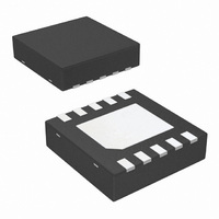
IC TEMP SENSOR DGTL REMOTE 10LLP
Manufacturer
National Semiconductor
Series
PowerWise®, TruTherm®r
Datasheet
1.LM96163CISDNOPB.pdf
(42 pages)
Specifications of LM96163CISD/NOPB
Function
Fan Control, Temp Monitor
Topology
ADC (Sigma Delta), Comparator, Register Bank, Tach
Sensor Type
External & Internal
Sensing Temperature
-40°C ~ 85°C, External Sensor
Output Type
SMBus™
Output Alarm
Yes
Output Fan
Yes
Voltage - Supply
3 V ~ 3.6 V
Operating Temperature
-40°C ~ 85°C
Mounting Type
Surface Mount
Package / Case
10-LLP
Temperature Sensor Function
Temp Sensor
Interface Type
Serial (2-Wire)
Resolution
10+SignBit
Package Type
LLP EP
Operating Temperature (min)
-40C
Operating Temperature (max)
85C
Operating Supply Voltage (min)
3V
Operating Supply Voltage (typ)
3.3V
Operating Supply Voltage (max)
3.6V
Lead Free Status / RoHS Status
Lead free / RoHS Compliant
Other names
LM96163CISDTR
Available stocks
Company
Part Number
Manufacturer
Quantity
Price

Part Number:
LM96163CISD/NOPB
Manufacturer:
TI/德州仪器
Quantity:
20 000


www.national.com
f
t
t
t
t
t
t
t
t
t
t
t
t
SMB
LOW
HIGH
R
F
OF
TIMEOUT
SU:DAT
HD:DAT
HD:STA
SU:STO
SU:STA
BUF
Symbol
SMBus Digital Switching Characteristics
Unless otherwise noted, these specifications apply for V
pF. Boldface limits apply for T
characteristics of the LM96163 fully meet or exceed the published specifications of the SMBus version 2.0. The following param-
eters are the timing relationships between SMBCLK and SMBDAT signals related to the LM96163. They adhere to but are not
necessarily the same as the SMBus bus specifications.
Note 1: Absolute Maximum Ratings indicate limits beyond which damage to the device may occur. Operating Ratings indicate conditions for which the device is
functional, but do not guarantee performance limits. For guaranteed specifications and test conditions, see the Electrical Characteristics. The guaranteed
specifications apply only for the test conditions listed. Some performance characteristics may degrade when the device is not operated under the listed test
conditions.
Note 2: All voltages are measured with respect to GND, unless otherwise noted.
Note 3: When the input voltage (V
components and/or ESD protection circuitry are shown below for the LM96163's pins. Care should be taken not to forward bias the parasitic diode, D2, present
on pins D+ and D−. Doing so by more than 50 mV may corrupt temperature measurements.
SMBus Clock Frequency
SMBus Clock Low Time
SMBus Clock High Time
SMBus Rise Time
SMBus Fall Time
Output Fall Time
SMBDAT and SMBCLK Time Low for Reset of
Serial Interface See
Data In Setup Time to SMBCLK High
Data Out Hold Time after SMBCLK Low
Hold Time after (Repeated) Start Condition. After
this period the first clock is generated.
Stop Condition SMBCLK High to SMBDAT Low
(Stop Condition Setup)
SMBus Repeated Start-Condition Setup Time,
SMBCLK High to SMBDAT Low
SMBus Free Time between Stop and Start
Conditions
IN
Parameter
) at any pin exceeds the power supplies (V
(Note
A
SMBus Timing Diagram for SMBCLK and SMBDAT Signals
= T
14)
J
; T
MIN
≤
T
A
≤
T
MAX
DD
; all other limits T
= +3.0 VDC to +3.6 VDC, C
From V
From V
(Note
(Note
C
L
= 400 pF, I
IN
6
< GND or V
12)
13)
IN(0) max
IN(1) min
A
O
IN
to V
to V
= T
= 3 mA
> V+), the current at that pin should be limited to 5 mA. Parasitic
Conditions
IN(1) min
J
IN(0) max
= +25°C, unless otherwise noted. The switching
L
(load capacitance) on output lines = 80
(Note
Limits
1075
100
250
250
300
100
4.7
4.0
0.3
4.0
4.7
4.7
10
50
25
35
1
9)
30041004
kHz (max)
kHz (min)
ms (max)
µs (max)
µs (max)
µs (max)
ns (max)
ms (min)
ns (max)
µs (min)
µs (min)
ns (min)
ns (min)
µs (min)
ns (min)
µs (min)
µs (min)
(Limit)
Units
Related parts for LM96163CISD/NOPB
Image
Part Number
Description
Manufacturer
Datasheet
Request
R

Part Number:
Description:
National Semiconductor [8-Bit D/A Converter]
Manufacturer:
National Semiconductor
Datasheet:
Part Number:
Description:
National Semiconductor [Media Coprocessor]
Manufacturer:
National Semiconductor
Datasheet:
Part Number:
Description:
Digitally Controlled Tone and Volume Circuit with Stereo Audio Power Amplifier, Microphone Preamp Stage and National 3D Sound
Manufacturer:
National Semiconductor
Datasheet:
Part Number:
Description:
Digitally Controlled Tone and Volume Circuit with Stereo Audio Power Amplifier, Microphone Preamp Stage and National 3D Sound
Manufacturer:
National Semiconductor
Datasheet:
Part Number:
Description:
AC97 Rev 2 Codec with Sample Rate Conversion and National 3D Sound
Manufacturer:
National Semiconductor
Part Number:
Description:
Manufacturer:
National Semiconductor
Datasheet:
Part Number:
Description:
Manufacturer:
National Semiconductor
Datasheet:
Part Number:
Description:
General Purpose, Low Voltage, Low Power, Rail-to-Rail Output Operational Amplifiers
Manufacturer:
National Semiconductor
Datasheet:
Part Number:
Description:
8-bit 20 MSPS flash A/D converter.
Manufacturer:
National Semiconductor
Datasheet:
Part Number:
Description:
Low Noise Quad Operational Amplifier
Manufacturer:
National Semiconductor
Datasheet:
Part Number:
Description:
Quad Differential Line Receivers
Manufacturer:
National Semiconductor
Datasheet:
Part Number:
Description:
Quad High Speed Trapezoidal? Bus Transceiver
Manufacturer:
National Semiconductor
Datasheet:
Part Number:
Description:
Dual Line Receiver
Manufacturer:
National Semiconductor
Datasheet:
Part Number:
Description:
TTL to 10k ECL Level Translator with Latch
Manufacturer:
National Semiconductor
Datasheet: