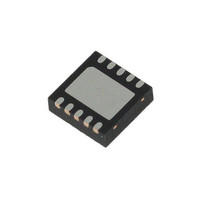
L6728DTR STMicroelectronics, L6728DTR Datasheet - Page 20

L6728DTR
Manufacturer Part Number
L6728DTR
Description
IC PWM CTLR 1PH POWERGOOD 10DFN
Manufacturer
STMicroelectronics
Datasheet
1.L6728DTR.pdf
(33 pages)
Specifications of L6728DTR
Pwm Type
Voltage Mode
Number Of Outputs
1
Frequency - Max
330kHz
Duty Cycle
80%
Voltage - Supply
5 V ~ 12 V
Buck
Yes
Boost
No
Flyback
No
Inverting
No
Doubler
No
Divider
No
Cuk
No
Isolated
No
Operating Temperature
-40°C ~ 125°C
Package / Case
10-DFN
Frequency-max
330kHz
Duty Cycle (max)
80 %
Mounting Style
SMD/SMT
Switching Frequency
300 KHz
Operating Supply Voltage
5 V to 12 V
Supply Current
6 mA
Lead Free Status / RoHS Status
Lead free / RoHS Compliant
Other names
497-10432-2
Available stocks
Company
Part Number
Manufacturer
Quantity
Price
Application information
11
11.1
20/33
Application information
Inductor design
The inductance value is defined by a compromise between the dynamic response time, the
efficiency, the cost and the size. The inductor has to be calculated to maintain the ripple
current (ΔI
value can be calculated with the following equation:
Where F
voltage.
inductor, with V
Increasing the value of the inductance reduces the current ripple but, at the same time,
increases the converter response time to a dynamic load change. The response time is the
time required by the inductor to change its current from initial to final value. Until the inductor
has finished its charging time, the output current is supplied by the output capacitors.
Minimizing the response time can minimize the output capacitance required. If the
compensation network is well-designed, during a load variation the device is able to set a
duty cycle value very different (0% or 80%) from a steady-state one. When this condition is
reached, the response time is limited by the time required to change the inductor current.
Figure 9.
L
=
V
----------------------------- -
F
IN
SW
–
Figure 9
SW
V
⋅
L
ΔI
OUT
) between 20% and 30% of the maximum output current (typ). The inductance
is the switching frequency, V
Inductor current ripple vs output voltage
L
⋅
IN
V
--------------
V
shows the ripple current vs. the output voltage for different values of the
OUT
= 5 V and V
IN
IN
Doc ID 16498 Rev 1
= 12 V.
IN
is the input voltage and V
OUT
is the output
L6728D


