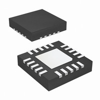
ISL6420BIRZ-TK Intersil, ISL6420BIRZ-TK Datasheet - Page 15

ISL6420BIRZ-TK
Manufacturer Part Number
ISL6420BIRZ-TK
Description
IC CTRLR PWM SYNC BUCK 20-QFN
Manufacturer
Intersil
Datasheet
1.ISL6420BIAZ-TK.pdf
(21 pages)
Specifications of ISL6420BIRZ-TK
Pwm Type
Voltage Mode
Number Of Outputs
1
Frequency - Max
1.4MHz
Duty Cycle
100%
Voltage - Supply
4.5 V ~ 28 V
Buck
Yes
Boost
No
Flyback
No
Inverting
No
Doubler
No
Divider
No
Cuk
No
Isolated
No
Operating Temperature
-40°C ~ 85°C
Package / Case
20-VQFN Exposed Pad, 20-HVQFN, 20-SQFN, 20-DHVQFN
Frequency-max
1.4MHz
Lead Free Status / RoHS Status
Lead free / RoHS Compliant
The slew time of the current is set by an external
capacitor on the CDEL pin, which is charged and
discharged with a 100µA current source. The change in
voltage on the capacitor is 2.5V. This same capacitor is
used to set the PGOOD active delay after soft-start.
When PGOOD is low, the internal PGOOD circuitry uses
the capacitor and when PGOOD is high, the voltage
margining circuit uses the capacitor. The slew time for
voltage margining can be in the range of 300µs to
2ms.
External Reference/DDR Supply
The voltage margining can be disabled by connecting
the VMSET/MODE to VCC5. In this mode, the chip can
be configured to work with an external reference input
and provide a buffered reference output.
If VMSET/MODE pin and the GPIO1/REFIN pin are both
tied to VCC5, then the internal 0.6V reference is used
as the error amplifier non-inverting input. The buffered
reference output on REFOUT will be 0.6V ±0.01V,
capable of sourcing 20mA and sinking up to 50µA
current with a 2.2µF capacitor connected to the
REFOUT pin.
If the VMSET/MODE pin is tied to high but
GPIO1/REFIN is connected to an external voltage
source between 0.6V to 1.25V, then this external
voltage is used as the reference voltage at the positive
input of the error amplifier. The buffered reference
output on REFOUT will be Vrefin ±0.01V, capable of
sourcing 20mA and sinking up to 50µA current with a
2.2µF capacitor on the REFOUT pin.
Power-Good
The PGOOD pin can be used to monitor the status of
the output voltage. PGOOD will be true (open drain)
when the FB pin is within ±10% of the reference and
the ENSS pin has completed its soft-start ramp.
Additionally, a capacitor on the CDEL pin will set a
delay for the PGOOD signal. After the ENSS pin
completes its soft-start ramp, a 2µA current begins
charging the CDEL capacitor to 2.5V. The capacitor will
be quickly discharged before PGOOD goes high. The
programmable delay can be used to sequence multiple
converters or as a LOW-true reset signal.
If the voltage on the FB pin exceeds ±10% of the
reference, then PGOOD will go low after 1µs of noise
filtering.
Over-Temperature Protection
The IC is protected against over-temperature
conditions. When the junction temperature exceeds
+150°C, the PWM shuts off. Normal operation is
resumed when the junction temperature is cooled
down to +130°C.
15
ISL6420B
Shutdown
When ENSS pin is below 1V, the regulator is disabled
with the PWM output drivers tri-stated. When disabled,
the IC power will be reduced.
Undervoltage
If the voltage on the FB pin is less than 15% of the
reference voltage for 8 consecutive PWM cycles, then
the circuit enters into soft-start hiccup mode. This
mode is identical to the overcurrent hiccup mode.
Overvoltage Protection
If the voltage on the FB pin exceeds the reference
voltage by 15%, the lower gate driver is turned on
continuously to discharge the output voltage. If the
overvoltage condition continues for 32 consecutive
PWM cycles, then the chip is turned off with the gate
drivers tri-stated. The voltage on the FB pin will fall
and reach the 15% undervoltage threshold. After 8
clock cycles, the chip will enter soft-start hiccup
mode. This mode is identical to the overcurrent hiccup
mode.
Gate Control Logic
The gate control logic translates generated PWM
control signals into the MOSFET gate drive signals
providing necessary amplification, level shifting and
shoot-through protection. Also, it has functions that
help optimize the IC performance over a wide range of
operational conditions.
Since MOSFET switching time can vary dramatically
from type to type and with the input voltage, the gate
control logic provides adaptive dead time by
monitoring the gate-to-source voltages of both upper
and lower MOSFETs. The lower MOSFET is not turned
on until the gate-to-source voltage of the upper
MOSFET has decreased to less than approximately 1V.
Similarly, the upper MOSFET is not turned on until the
gate-to-source voltage of the lower MOSFET has
decreased to less than approximately 1V. This allows a
wide variety of upper and lower MOSFETs to be used
without a concern for simultaneous conduction, or
shoot-through.
Start-up into Pre-Biased Load
The ISL6420B is designed to power-up into a
pre-biased load. This is achieved by transitioning from
Diode Emulation mode to a Forced Continuous
Conduction mode during start-up. The lower gate turns
ON for a short period of time and the voltage on the
phase pin is sensed. When this goes negative the lower
gate is turned OFF and remains OFF till the next cycle.
As a result, the inductor current will not go negative
during soft-start and thus will not discharge the
pre-biased load. The waveform for this condition is
shown in Figure 14.
December 4, 2009
FN6901.1


