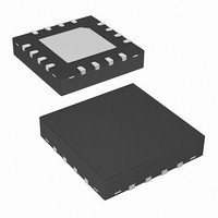
ISL8106CRZ Intersil, ISL8106CRZ Datasheet

ISL8106CRZ
Specifications of ISL8106CRZ
Available stocks
Related parts for ISL8106CRZ
ISL8106CRZ Summary of contents
Page 1
... CAUTION: These devices are sensitive to electrostatic discharge; follow proper IC Handling Procedures. 1-888-INTERSIL or 1-888-468-3774 ISL8106 FN9283.1 3 technology delivers extremely fast -0.3V CC DS(ON) | Intersil (and design registered trademark of Intersil Americas Inc. Copyright Intersil Americas Inc. 2006. All Rights Reserved All other trademarks mentioned are the property of their respective owners. ...
Page 2
... Ordering Information PART NUMBER ISL8106CRZ* ISL8106IRZ* ISL8106EVAL1Z *Add “-T” suffix for tape and reel. NOTE: Intersil Pb-free plus anneal products employ special Pb-free material sets; molding compounds/die attach materials and 100% matte tin plate termination finish, which are RoHS compliant and compatible with both SnPb and Pb-free soldering operations. Intersil Pb-free products are MSL classified at Pb-free peak reflow temperatures that meet or exceed the Pb-free requirements of IPC/JEDEC J STD-020 ...
Page 3
Block Diagram VIN GND PACKAGE BOTTOM VCC V REF EN − OVP + − UVP + + EA EA − FB COMP − BSOC OCP 30Ω PGOOD LDO PWM FREQUENCY + − + ...
Page 4
... Thermal Information Thermal Resistance (Typical, Notes 1, 2) θ QFN Package . . . . . . . . . . . . . . . . . . . Junction Temperature Range . . . . . . . . . . . . . . . . . -55°C to +150°C Operating Temperature Range ISL8106CRZ 0°C to +70°C ISL8106IRZ . . . . . . . . . . . . . . . . . . . . . . . . . . . . -40°C to +85°C Storage Temperature . . . . . . . . . . . . . . . . . . . . . . . -65°C to +150°C Lead Temperature . . . . . . . . . . . . . . . . . . . . (soldering, 10s)+300°C Recommended Operating Conditions Ambient Temperature Range (ISL8106C 0° ...
Page 5
... V F PVCC = 5V 2mA 25V PGR SS PGOOD = 5mA Sink; ISL8106CRZ PGR UV PGR SS PGOOD = 5mA Sink; ISL8106IRZ PGR UV PGR OV PGOOD = 5mA Sink; ISL8106CRZ PGOOD = 5mA Sink; ISL8106IRZ PGR OC PGOOD = 5mA Sink; ISL8016CRZ PGOOD = 5mA Sink; ISL8106IRZ I PGOOD PGOOD = 5V MIN TYP MAX UNIT 200 ...
Page 6
... The EN pin is the on/off switch of the IC. When the EN pin is pulled above the rising threshold voltage V ramp up and begin regulation. The soft-start sequence begins once V ramps above the power-on reset (POR ISL8106 SYMBOL TEST CONDITIONS High to PGOOD High; ISL8106CRZ EN High to PGOOD High; ISL8106IRZ I OC ISL8106CRZ ISL8106IRZ OVR V OVF T OTR (Note 3) ...
Page 7
PGND (Pin 10) The PGND pin should be connected to the source of the bottom-side MOSFET, preferably with an isolated path that is in parallel with the trace connecting the BGATE pin to the gate of the MOSFET. The PGND ...
Page 8
... VIN pin; the CC LDO has no pull-down capability. Pulse Width Modulator The ISL8106 is a hybrid of fixed frequency PWM control, and variable frequency hysteretic control. Intersil’ ISL8106 can simultaneously affect the PWM switching frequency and PWM duty cycle in response to input voltage and output load transients. The term “ ...
Page 9
MOSFET Gate-Drivers The ISL8106 has internal gate-drivers for the top-side and bottom-side N-Channel MOSFETs. The bottom-side gate- driver is optimized for low duty-cycle applications where the bottom-side MOSFET conduction losses are dominant, requiring a low r MOSFET. The BGATE pulldown ...
Page 10
Where (Ω) is the resistor used to program the over- BSOC current setpoint - I is the current sense current that is sourced from BSOC the BSOC pin - I is the I threshold current value sourced from ...
Page 11
Keep the metal runs from the LX terminals to the output inductor short. The power plane should support the input power and output power nodes. Use copper filled polygons on the top and bottom circuit layers for the LX ...
Page 12
ESR to achieve the required V The inductance of the capacitor can cause a brief voltage dip when the load transient has an extremely high slew rate. Low inductance capacitors constructed with reverse package geometry are ...
Page 13
For the top-side MOSFET, its switching loss can be written as • • • IN VAL ON OSC ( ) ------------------------------------------------------------ - SWTS IN 2 The peak and valley current of the ...
Page 14
... COMP COMP1 COMP2 The Your local Intersil representative can provide a PC- based tool that can be used to calculate compensation network component values and help simulate the loop frequency response. The compensation network consists of the internal error amplifier of the ISL8106 and the external ...
Page 15
... Accordingly, the reader is cautioned to verify that data sheets are current before placing orders. Information furnished by Intersil is believed to be accurate and reliable. However, no responsibility is assumed by Intersil or its subsidiaries for its use; nor for any infringements of patents or other rights of third parties which may result from its use ...


