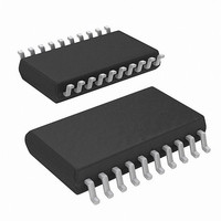
ISL6754AAZA Intersil, ISL6754AAZA Datasheet - Page 15

ISL6754AAZA
Manufacturer Part Number
ISL6754AAZA
Description
IC CTRLR PWM FULL-BRDG 20-QSOP
Manufacturer
Intersil
Datasheet
1.ISL6754AAZA-T.pdf
(19 pages)
Specifications of ISL6754AAZA
Pwm Type
Voltage/Current Mode
Number Of Outputs
6
Frequency - Max
2MHz
Duty Cycle
100%
Voltage - Supply
9 V ~ 16 V
Buck
No
Boost
No
Flyback
No
Inverting
No
Doubler
No
Divider
No
Cuk
No
Isolated
No
Operating Temperature
-40°C ~ 105°C
Package / Case
20-QSOP
Frequency-max
2MHz
Lead Free Status / RoHS Status
Lead free / RoHS Compliant
Available stocks
Company
Part Number
Manufacturer
Quantity
Price
Company:
Part Number:
ISL6754AAZA
Manufacturer:
Intersil
Quantity:
522
Company:
Part Number:
ISL6754AAZA-T
Manufacturer:
Intersil
Quantity:
1 900
Using CT to provide slope compensation instead of CTBUF
requires the same calculations, except that Equations 22
and 23 require modification. Equation 22 becomes:
and Equation 23 becomes:
R9
The buffer transistor used to create the external ramp from
CT should have a sufficiently high gain (>200) so as to
minimize the required base current. Whatever base current
is required reduces the charging current into CT and will
reduce the oscillator frequency.
ZVS Full-Bridge Operation
The ISL6754 is a full-bridge zero-voltage switching (ZVS)
PWM controller that behaves much like a traditional hard-
switched topology controller. Rather than drive the diagonal
bridge switches simultaneously, the upper switches (OUTUL,
OUTUR) are driven at a fixed 50% duty cycle and the lower
switches (OUTLL, OUTLR) are pulse width modulated on
the trailing edge.
V
e
FIGURE 11. ADDING SLOPE COMPENSATION USING CT
–
=
ΔV
(
------------------------------------------------------------ -
2D V
CS
–
=
V
e
e
--------------------- -
R6
2D R6
–
+
ΔV
R
ΔV
+
⋅
CS
R9
CS
CS
) R6
⋅
R9
C4
R6
V
15
Ω
10
CT
1
2
3
4
5
6
7
8
9
VREF
CT
RAMP
CS
ISL6754
GND
(EQ. 25)
(EQ. 26)
20
19
18
17
16
15
14
13
12
11
ISL6754
To understand how the ZVS method operates one must
include the parasitic elements of the circuit and examine a
full switching cycle.
In Figure 13, the power semiconductor switches have been
replaced by ideal switch elements with parallel diodes and
capacitance, the output rectifiers are ideal, and the
transformer leakage inductance has been included as a
discrete element. The parasitic capacitance has been
lumped together as switch capacitance, but represents all
parasitic capacitance in the circuit including winding
capacitance. Each switch is designated by its position, upper
left (UL), upper right (UR), lower left (LL), and lower right
(LR). The beginning of the cycle, shown in Figure 14, is
arbitrarily set as having switches UL and LR on and UR and
LL off. The direction of the primary and secondary currents
are indicated by I
VIN+
VIN+
VIN-
VIN-
DEADTIME
OUTUR
OUTLR
OUTUL
OUTLL
UL
UL
LL
LL
CT
FIGURE 14. UL - LR POWER TRANSFER CYCLE
FIGURE 12. BRIDGE DRIVE SIGNAL TIMING
FIGURE 13. IDEALIZED FULL-BRIDGE
I
P
PWM
P
and I
UR
LR
UR
LR
L
L
S
L
L
, respectively.
WINDOW
RESDEL
PWM
D1
D2
D1
D2
RESONANT
DELAY
PWM
I
S
September 29, 2008
PWM
FN6754.1
VOUT+
VOUT+
RTN
RTN


