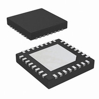
ISL9440BIRZ-T Intersil, ISL9440BIRZ-T Datasheet - Page 9

ISL9440BIRZ-T
Manufacturer Part Number
ISL9440BIRZ-T
Description
IC CTRLR PWM OUT-OF-PHASE 32-QFN
Manufacturer
Intersil
Datasheet
1.ISL9440BIRZ.pdf
(24 pages)
Specifications of ISL9440BIRZ-T
Pwm Type
Current Mode
Number Of Outputs
4
Frequency - Max
340kHz
Duty Cycle
93%
Voltage - Supply
4.5 V ~ 24 V
Buck
Yes
Boost
No
Flyback
No
Inverting
No
Doubler
No
Divider
No
Cuk
No
Isolated
No
Operating Temperature
-40°C ~ 85°C
Package / Case
32-VQFN Exposed Pad, 32-HVQFN, 32-SQFN, 32-DHVQFN
Frequency-max
340kHz
Lead Free Status / RoHS Status
Lead free / RoHS Compliant
Available stocks
Company
Part Number
Manufacturer
Quantity
Price
Company:
Part Number:
ISL9440BIRZ-T
Manufacturer:
Intersil
Quantity:
6 000
Pin Descriptions
BOOT3, BOOT2, BOOT1 (Pin 20, 26, 31)
These pins are bootstrap pins to provide bias for high side
driver. The bootstrap diodes are integrated to help reduce
total cost and reduce layout complexity.
UGATE3, UGATE2, UGATE1 (Pins 21, 27, 30)
These pins provide the gate drive for the upper MOSFETs.
PHASE3, PHASE2, PHASE1 (Pins 19, 25, 32)
These pins are connected to the junction of the upper
MOSFETs source, output filter inductor, and lower MOSFETs
drain.
LGATE3, LGATE2, LGATE1 (Pins 22, 28, 29)
These pins provide the gate drive for the lower MOSFETs.
PGND (Pin 23)
This pin provides the power ground connection for the lower
gate drivers for all PWM1, PWM2 and PWM3. This pin
should be connected to the sources of the lower MOSFETs
and the (-) terminals of the external input capacitors.
FB3, FB2, FB1, LDOFB (Pin 16, 13, 6, 10)
These pins are connected to the feedback resistor divider
and provide the voltage feedback signals for the respective
controller. They set the output voltage of the converter. In
addition, the PGOOD circuit uses these inputs to monitor the
output voltage status.
ISEN3, ISEN2, ISEN1 (Pin 18, 24, 1)
These pins are used to monitor the voltage drop across the
lower MOSFET for current loop feedback and overcurrent
protection.
PGOOD (Pin 2)
This is an open drain logic output used to indicate the status
of the output voltages AND input voltage. This pin is pulled
low when any of the three PWM outputs is not within 10% of
the respective nominal voltage, or if the linear controller
output is less than 75% of its nominal value, or VIN pin
voltage drops below 5.55V.
The PGOOD pin also indicates the VIN pin status for early
warning function. If the voltage on VIN pin drops below
5.55V, this pin will be pulled low.
SGND (Pin 11)
This is the small-signal ground, common to all 4 controllers,
and is suggested to be routed separately from the high
current ground (PGND). In case of one whole solid ground
and no noisy current going through around chip, SGND and
PGND can be tied to the same ground copper plane. All
voltage levels are measured with respect to this pin. A small
ceramic capacitor should be connected right next to this pin
for noise decoupling.
9
ISL9440B, ISL9440C
VIN (Pin 4)
Use this pin to power the device with an external supply
voltage with a range of 5.6V to 24V. For 5V ±10% operation,
connect this pin to VCC_5V.
For ISL9440B and ISL9440C, the voltage on this pin is
monitored for early warning function. If the voltage on this
pin drop below 5.55V, the PGOOD will be pulled low. RST
will be low after PGOOD toggles to low for 5.5µs (TYP).
Refer to Figure 1 for detailed time sequence.
VCC_5V (Pin 3)
This pin is the output of the internal 5V linear regulator. This
output supplies the bias for the IC, the low-side gate drivers,
and the external boot circuitry for the high-side gate drivers.
The IC may be powered directly from a single 5V (±10%)
supply at this pin. When used as a 5V supply input, this pin
must be externally connected to V
be always decoupled to power ground with a minimum of
4.7µF ceramic capacitor, placed very close to the pin.
EN/SS3, EN/SS2, EN/SS1 (Pin 17, 14, 5)
These pins provide an enable/disable function and soft
starting for their respective PWM outputs. The output is
disabled when the pin is pulled to GND. When a capacitor is
connected from one of these pins to the ground, a regulated
1.55µA soft-start current charges this capacitor during soft
starting. When the voltage on the EN/SSx pin reaches 1.3V,
the corresponding PWM output is active. From 1.3V to 2.1V,
the reference voltage of the corresponding PWM channel is
clamped to the voltage at EN/SSx minus 1.3V. The
capacitance of the soft-start capacitors sets the soft-starting
time and enable delay time. Setting the soft-starting time too
short might create undesirable overshoot at the output
during start-up. It is recommended that the soft-starting time
be greater than 1.0ms. Please do not float this pin.
The typical soft-start time is set according to Equation 1:
G4 (Pin 9)
This pin is the open drain output of the linear regulator
controller.
OCSET3, OCSET2, OCSET1 (Pin 15, 12, 7)
A resistor from this pin to ground sets the overcurrent
threshold for the respective PWM.
RST (Pin 8)
Reset pulse output. This pin outputs a logic LOW signal after
PGOOD toggles to low for 5.5µs (TYP). It can be used to
reset system.
Refer to Figure 1 for detailed time sequence with early
warning function.
t
SSx
=
0.8V
⎛
⎝
------------------- -
1.55μA
C
SSx
⎞
⎠
IN
. The VCC_5V pin must
June 24, 2010
FN6799.3
(EQ. 1)


