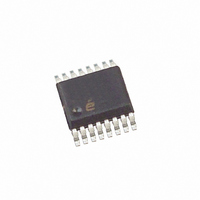
ISL6753AAZA Intersil, ISL6753AAZA Datasheet

ISL6753AAZA
Specifications of ISL6753AAZA
Available stocks
Related parts for ISL6753AAZA
ISL6753AAZA Summary of contents
Page 1
... Ordering Information PART PART TEMP. NUMBER MARKING RANGE (°C) PACKAGE ISL6753AAZA ISL6753AAZ -40 to 105 (See Note) Add -T suffix to part number for tape and reel packaging NOTE: Intersil Pb-free plus anneal products employ special Pb-free material sets; molding compounds/die attach materials and 100% matte tin plate termination finish, which are RoHS compliant and compatible with both SnPb and Pb-free soldering operations ...
Page 2
Functional Block Diagram VDD VREF UVLO OVER- TEMPERATURE PROTECTION GND VREF RESDEL OSCILLATOR CT RTD CTBUF SS 50% PWM STEERING LOGIC PWM + - 1.00V OVER CURRENT COMPARATOR 80mV + - 0.33 PWM COMPARATOR VREF SOFTSTART CONTROL VDD OUTUL OUTUR ...
Page 3
Typical Application - High Voltage Input ZVS Full-Bridge Converter P1 VIN+ Q1 FQB6N50 3 Q6 BSS138LT1 1 R13 2 10.0k R14 CR3 4. SS12 0805 C1-C4 33uF 450V + + R1 300 - 400 4.7k VDC 5% 2512 ...
Page 4
Absolute Maximum Ratings Supply Voltage, VDD . . . . . . . . . . . . . . . . . . . GND - 0.3V to +20.0V OUTxxx . . . . . . . . . ...
Page 5
Electrical Specifications Recommended operating conditions unless otherwise noted. Refer to Block Diagram and Typical Application schematic. 9V < VDD < 20V, RTD = 10.0kΩ 470pF 25°C (Continued) A PARAMETER Bias Current Clamp Voltage PULSE WIDTH ...
Page 6
Electrical Specifications Recommended operating conditions unless otherwise noted. Refer to Block Diagram and Typical Application schematic. 9V < VDD < 20V, RTD = 10.0kΩ 470pF 25°C (Continued) A PARAMETER CTBUF VOL SOFT-START Charging Current SS ...
Page 7
Typical Performance Curves 1.02 1.01 1 0.99 0. 110 Temperature (C) FIGURE 1. REFERENCE VOLTAGE vs TEMPERATURE 100 ...
Page 8
For current-mode control this pin is connected to CS and the current loop feedback signal is applied to both inputs. For voltage-mode control, the oscillator sawtooth waveform may be buffered and used to generate ...
Page 9
Soft-Start Operation The ISL6753 features a soft-start using an external capacitor in conjunction with an internal current source. Soft-start reduces component stresses and surge currents during start-up. Upon start-up, the soft-start circuitry limits the error voltage input (VERR ...
Page 10
The charging time of the ramp capacitor is RAMP PEAK ⋅ ⋅ --------------------------------------- - – – MIN For optimum performance, the ...
Page 11
For simplicity, idealized components have been used for this discussion, but the effect of magnetizing inductance must be considered when determining the amount of external ramp to add. Magnetizing inductance provides a degree of slope compensation to the current feedback ...
Page 12
If the application requires deadtime less than about 500ns, the CTBUF signal may not perform adequately for slope compensation. CTBUF lags the CT sawtooth waveform by 300-400ns. This behavior results in a non-zero value of CTBUF when the next half-cycle ...
Page 13
VIN VIN- FIGURE 11 POWER TRANSFER CYCLE The power transfer period terminates when switch LR turns off as determined by the PWM. The current ...
Page 14
The second power transfer period commences when switch LL closes. With switches UR and LL on, the primary and secondary currents flow as indicated below. VIN VIN- FIGURE 14 ...
Page 15
... Accordingly, the reader is cautioned to verify that data sheets are current before placing orders. Information furnished by Intersil is believed to be accurate and reliable. However, no responsibility is assumed by Intersil or its subsidiaries for its use; nor for any infringements of patents or other rights of third parties which may result from its use ...


