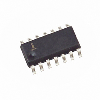
ISL6439CB-T Intersil, ISL6439CB-T Datasheet - Page 7

ISL6439CB-T
Manufacturer Part Number
ISL6439CB-T
Description
IC CNTRLR PWM SYNC BUCK 14-SOIC
Manufacturer
Intersil
Datasheet
1.ISL6439CB.pdf
(15 pages)
Specifications of ISL6439CB-T
Pwm Type
Voltage Mode
Number Of Outputs
1
Frequency - Max
325kHz
Duty Cycle
100%
Voltage - Supply
3.3 V ~ 5 V
Buck
Yes
Boost
No
Flyback
No
Inverting
No
Doubler
No
Divider
No
Cuk
No
Isolated
No
Operating Temperature
0°C ~ 70°C
Package / Case
14-SOIC (3.9mm Width), 14-SOL
Frequency-max
325kHz
Lead Free Status / RoHS Status
Contains lead / RoHS non-compliant
CT1 and CT2
These pins are the connections for the external charge
pump capacitor. A minimum of a 0.1μF ceramic capacitor is
recommended for proper operation of the IC.
CPVOUT
This pin represents the output of the charge pump. The
voltage at this pin is the bias voltage for the IC. Connect a
decoupling capacitor from this pin to ground. The value of
the decoupling capacitor should be at least 10x the value of
the charge pump capacitor. This pin may be tied to the
bootstrap circuit as the source for creating the BOOT
voltage.
CPGND
This pin represents the signal and power ground for the
charge pump. Tie this pin to the ground island/plane through
the lowest impedance connection available.
Functional Description
Initialization
The ISL6439 automatically initializes upon receipt of power.
Special sequencing of the input supplies is not necessary.
The Power-On Reset (POR) function continually monitors the
the output voltage of the charge pump. During POR, the charge
pump operates on a free running oscillator. Once the POR level
is reached, the charge pump oscillator is synched to the PWM
oscillator. The POR function also initiates the soft-start
operation after the charge pump output voltage exceeds its
POR threshold.
Soft-Start
The POR function initiates the digital soft-start sequence. The
PWM error amplifier reference is clamped to a level
proportional to the soft-start voltage. As the soft-start voltage
slews up, the PWM comparator generates PHASE pulses of
increasing width that charge the output capacitor(s). This
method provides a rapid and controlled output voltage rise. The
soft start sequence typically takes about 6.5ms.
0V
(1V/DIV)
FIGURE 1. SOFT-START INTERVAL
T0
T1
T2
TIME
7
T3
CPVOUT (5V)
V
VCC (3.3V)
OUT
(2.50V)
ISL6439, ISL6439A
Figure 1 shows the soft-start sequence for a typical application.
At t0, the +3.3V VCC voltage starts to ramp. At time t1, the
Charge Pump begins operation and the +5V CPVOUT IC bias
voltage starts to ramp up. Once the voltage on CPVOUT
crosses the POR threshold at time t2, the output begins the
soft-start sequence. The triangle waveform from the PWM
oscillator is compared to the rising error amplifier output
voltage. As the error amplifier voltage increases, the pulse-
width on the UGATE pin increases to reach the steady-state
duty cycle at time t3.
Shoot-Through Protection
A shoot-through condition occurs when both the upper
MOSFET and lower MOSFET are turned on simultaneously,
effectively shorting the input voltage to ground. To protect
the regulator from a shoot-through condition, the ISL6439
incorporates specialized circuitry which insures that the
complementary MOSFETs are not ON simultaneously.
The adaptive shoot-through protection utilized by the
ISL6439 looks at the lower gate drive pin, LGATE, and the
upper gate drive pin, UGATE, to determine whether a
MOSFET is ON or OFF. If the voltage from UGATE or from
LGATE to GND is less than 0.8V, then the respective
MOSFET is defined as being OFF and the complementary
MOSFET is turned ON. This method of shoot-through
protection allows the regulator to sink or source current.
Since the voltage of the lower MOSFET gate and the upper
MOSFET gate are being measured to determine the state of
the MOSFET, the designer is encouraged to consider the
repercussions of introducing external components between
the gate drivers and their respective MOSFET gates before
actually implementing such measures. Doing so may
interfere with the shoot-through protection.
Output Voltage Selection
The output voltage can be programmed to any level between
V
divider is used to scale the output voltage relative to the
reference voltage and feed it back to the inverting input of
the error amplifier, see Figure 2. However, since the value of
R1 affects the values of the rest of the compensation
components, it is advisable to keep its value less than 5kΩ.
R4 can be calculated based on Equation 2:
If the output voltage desired is 0.8V, simply route the output
back to the FB pin through R1, but do not populate R4.
Overcurrent Protection
The overcurrent function protects the converter from a shorted
output by using the upper MOSFET on-resistance, r
monitor the current. This method enhances the converter’s
efficiency and reduces cost by eliminating a current sensing
resistor.
R4
IN
and the internal reference, 0.8V. An external resistor
=
------------------------------------- -
V
OUT1
R1 0.8V
×
–
0.8V
November 5, 2008
DS(ON)
FN9057.5
(EQ. 2)
, to


