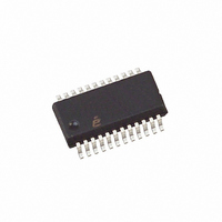
ISL6442IA Intersil, ISL6442IA Datasheet - Page 8

ISL6442IA
Manufacturer Part Number
ISL6442IA
Description
IC PWM BUCK VM 24QSOP
Manufacturer
Intersil
Datasheet
1.ISL6442IAZ-TK.pdf
(16 pages)
Specifications of ISL6442IA
Pwm Type
Voltage Mode
Number Of Outputs
3
Frequency - Max
2.85MHz
Duty Cycle
100%
Voltage - Supply
4.5 V ~ 24 V
Buck
Yes
Boost
No
Flyback
No
Inverting
No
Doubler
No
Divider
No
Cuk
No
Isolated
No
Operating Temperature
-40°C ~ 85°C
Package / Case
24-QSOP
Frequency-max
2.85MHz
Lead Free Status / RoHS Status
Contains lead / RoHS non-compliant
Available stocks
Company
Part Number
Manufacturer
Quantity
Price
Company:
Part Number:
ISL6442IAZ
Manufacturer:
Intersil
Quantity:
97
Company:
Part Number:
ISL6442IAZ
Manufacturer:
ST
Quantity:
6 267
Part Number:
ISL6442IAZ
Manufacturer:
INTERSIL
Quantity:
20 000
Part Number:
ISL6442IAZ-T
Manufacturer:
INTERSIL
Quantity:
20 000
Company:
Part Number:
ISL6442IAZ-TK
Manufacturer:
Intersil
Quantity:
6 000
released. Then both 30µA current sources will start charging
up both capacitors in parallel. Once the voltage on both of
these pins is above 1.0V, this internal switch is turned off and
each 30µA internal current source charges its corresponding
soft-start capacitor connected to its soft-start pin. The
charging continues until the voltage across the soft-start
capacitor reaches 3.2V. However, the output voltage reaches
its regulation value when the soft-start capacitor voltage
reaches 1.6V. Figure 5 shows the typical waveforms for
SS2/EN2 and VOUT2; SS1/EN1 and VOUT1 are similar.
The soft-start ramps for each output can be selected
independently, but the ISL6442 also has voltage tracking
capability. By selecting the soft-start capacitance to be
proportional to the output voltage, the output voltage can be
tracked. For example, in Figure 6, SS1 capacitor = 0.18µF
and SS2 capacitor = 0.33µF, which match the output voltage
ratio (1.8V and 3.3V). Therefore, the lower VOUT1 ramp will
track with the VOUT2 ramp until they both reach 1.8V;
VOUT1 then levels off, while VOUT2 continues rising
towards 3.3V.
The basic timing equation is shown in Equation 2:
where:
t is the charge time
C is the external capacitance
dV is the voltage charged
I is the charging current (nominal 30µA)
t
GND>
GND>
=
C
•
dV
-------
I
FIGURE 5. SOFT-START
1.0V
SS2/EN2 (0.5V/DIV)
1.6V
8
VOUT2 (2V/DIV)
(EQ. 2)
ISL6442
From 0.0V to 1.0V, C = (C1 + C2 µF); dV = 1V; I = (30 + 30µA);
for a 0.1µF capacitor on each pin, t = 3.3ms. This time
represents the delay from when the soft-start ramp begins, until
the output voltage ramp begins.
Then, from 1.0V to 1.6V, the outputs will ramp individually
from zero to full-scale. Use the same equation to calculate the
time for each ramp; now if V = 0.6V, C = 0.1µF, and I = 30µA,
then t = 2ms.
Finally, there is a delay after 1.6V, until the ramp gets to
~3.2V, which signals that the ramp is done; when both ramps
are done, the PGOOD delay begins.
Figure 7 shows a typical power-up sequence. VIN turns on
and begins to ramp up; once VCC passes the rising POR trip
point, the linear output is enabled (with no soft-start ramp).
The SS1/EN1 pins also start charging (if not held low
externally); after a delay for them to reach 1V, VOUT1 and
VOUT2 begin to ramp; they are shown in tracking mode.
GND>
GND>
GND>
GND>
GND>
GND>
GND>
GND>
1.6V
1.0V
FIGURE 6. VOLTAGE TRACKING
FIGURE 7. OUTPUT VOLTAGES
SS1/EN1 (0.5V/DIV)
SS2/EN2 (0.5V/DIV)
VOUT1 (1V/DIV)
VOUT3 (1V/DIV)
VOUT2 (1V/DIV)
VOUT2 (1V/DIV)
VOUT (1V/DIV)
VIN (5V/DIV)
October 31, 2008
FN9204.2


