ISL6563IR Intersil, ISL6563IR Datasheet - Page 7
ISL6563IR
Manufacturer Part Number
ISL6563IR
Description
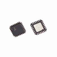
IC CNTRLR PWM 2-PH BUCK 24-QFN
Manufacturer
Intersil
Datasheet
1.ISL6563IR.pdf
(19 pages)
Specifications of ISL6563IR
Applications
Controller, Intel VRM9, VRM10, and AMD Hammer Applications
Voltage - Input
5 ~ 12 V
Number Of Outputs
1
Voltage - Output
0.8 ~ 1.85 V
Operating Temperature
-40°C ~ 85°C
Mounting Type
Surface Mount
Package / Case
24-VQFN Exposed Pad, 24-HVQFN, 24-SQFN, 24-DHVQFN
Lead Free Status / RoHS Status
Contains lead / RoHS non-compliant
Available stocks
Company
Part Number
Manufacturer
Quantity
Price
Company:

Part Number:
ISL6563IRZ
Manufacturer:
Intersil
Quantity:
300


For more information, refer to the ‘Output Voltage Offset
Programming’ paragraph.
SSEND (Pin 10)
This pin is an end of Soft-Start (SS) indicator; open drain
output device stays ON during soft-start, and goes open when
soft-start ends.
Operation
Figure 1 shows a simplified diagram of the voltage regulation
and current control loops. Both voltage and current feedback
are used to precisely regulate the output voltage and tightly
control the output currents, I
channels.
Voltage Loop
Feedback from the output voltage is applied via resistor R1
to the inverting input of the Error Amplifier. This signal can
drive the Error Amplifier output either high or low, depending
upon the output voltage. Low output voltage makes the
amplifier output move towards a higher output voltage level.
Amplifier output voltage is applied to the positive inputs of
the PWM Circuit comparators via the correction summing
networks. Out-of-phase sawtooth signals are applied to the
two PWM comparators inverting inputs. Increasing Error
Amplifier voltage results in increased Comparator output
duty cycle. This increased duty cycle signal is passed
COMP
R2
R1
C2
FB
FIGURE 1. SIMPLIFIED BLOCK DIAGRAM OF THE ISL6563 VOLTAGE AND CURRENT CONTROL LOOPS
SOURCE, I
DROOP
REFERENCE
ERROR
DAC
AMP
&
FB
L1
7
and I
Σ
L2
, of the two power
Σ
OSCILLATOR
Σ
Σ
AVERAGE
CIRCUIT
CIRCUIT
PWM
PWM
ISL6563
through the output drivers with no phase reversal to drive the
external upper MOSFETs. Increased duty cycle or ON time
for the upper MOSFET transistors results in increased
output voltage to compensate for the low output voltage
sensed.
Current Loop
The current control loop works in a similar fashion to the
voltage control loop, but with current control information
applied individually to each channel’s Comparator. The
information used for this control is the voltage that is
developed across the r
they are conducting. A single resistor converts and scales
the voltage across the MOSFETs to a current that is applied
to the Current Sensing circuit within the ISL6563. Output
from these sensing circuits is applied to the current
averaging circuit. Each PWM channel receives the
difference current signal from the summing circuit that
compares the average sensed current to the individual
channel current. When a power channel’s current is greater
than the average current, the signal applied via the summing
Correction circuit to the Comparator, reduces the output
pulse width of the Comparator to compensate for the
detected “above average” current in that channel.
Droop Implementation
In addition to controlling each channel’s output current, the
average channel current is used to implement an output
CURRENT
CURRENT
HALF-BRIDGE
HALF-BRIDGE
SENSE
SENSE
DRIVE
DRIVE
LGATE2
UGATE1
UGATE2
DS(ON)
LGATE1
PHASE1
PHASE2
ISEN
R
ISEN
of each lower MOSFET, while
V
V
IN
IN
VCC
L1
L2
June 10, 2010
C
V
OUT
FN9126.8
OUT
Related parts for ISL6563IR
Image
Part Number
Description
Manufacturer
Datasheet
Request
R

Part Number:
Description:
Intersil Corporation [CMOS Serial Controller Interface]
Manufacturer:
Intersil Corporation
Datasheet:
Part Number:
Description:
Manufacturer:
Intersil Corporation
Datasheet:
Part Number:
Description:
357-036-542-201 CARDEDGE 36POS DL .156 BLK LOPRO
Manufacturer:
Intersil Corporation
Datasheet:
Part Number:
Description:
1024-Word x 4-Bit LSI Static RAM
Manufacturer:
Intersil Corporation
Datasheet:
Part Number:
Description:
General Purpose NPN Transistor Arrays FN341.4
Manufacturer:
Intersil Corporation
Datasheet:
Part Number:
Description:
CMOS 16-Bit Microprocessor
Manufacturer:
Intersil Corporation
Datasheet:
Part Number:
Description:
Manufacturer:
Intersil Corporation
Datasheet:
Part Number:
Description:
Manufacturer:
Intersil Corporation
Datasheet:
Part Number:
Description:
Manufacturer:
Intersil Corporation
Datasheet:
Part Number:
Description:
Manufacturer:
Intersil Corporation
Datasheet:
Part Number:
Description:
CMOS 6-Bit Latch and Decoder Memory Interfaces
Manufacturer:
Intersil Corporation
Datasheet:
Part Number:
Description:
CA3046General Purpose NPN Transistor Arrays
Manufacturer:
Intersil Corporation
Datasheet:
Part Number:
Description:
Manufacturer:
Intersil Corporation
Datasheet:
Part Number:
Description:
TR909 DLC/FLC SLIC with Low Power Standby
Manufacturer:
Intersil Corporation
Datasheet:
Part Number:
Description:
Manufacturer:
Intersil Corporation
Datasheet: