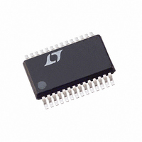
LTC1703CG#TRPBF Linear Technology, LTC1703CG#TRPBF Datasheet - Page 10

LTC1703CG#TRPBF
Manufacturer Part Number
LTC1703CG#TRPBF
Description
IC REG SW DUAL SYNC VID 28SSOP
Manufacturer
Linear Technology
Datasheet
1.LTC1703CG.pdf
(36 pages)
Specifications of LTC1703CG#TRPBF
Applications
Controller, Mobile Intel Pentium® III
Voltage - Input
3 ~ 7 V
Number Of Outputs
2
Voltage - Output
0.9 ~ 2 V
Operating Temperature
0°C ~ 85°C
Mounting Type
Surface Mount
Package / Case
28-SSOP
Lead Free Status / RoHS Status
Lead free / RoHS Compliant
Available stocks
Company
Part Number
Manufacturer
Quantity
Price
APPLICATIO S I FOR ATIO
LTC1703
of the equation—with a typical value on the order of 1µH,
the inductor allows very fast di/dt slew rates. The result is
superior transient response compared with conventional
solutions.
High Efficiency
The LTC1703 uses a synchronous step-down (buck)
architecture, with two external N-channel MOSFETs per
output. A floating topside driver and a simple external
charge pump provide full gate drive to the upper MOSFET.
The voltage mode feedback loop and MOSFET V
limit sensing remove the need for an external current
sense resistor, eliminating an external component and a
source of power loss in the high current path. Properly
designed circuits using low gate charge MOSFETs are
capable of efficiencies exceeding 90% over a wide range
of output voltages.
VID Programming
The LTC1703 includes an onboard feedback network that
programs the output voltage at side 1 in accordance with
the Intel Mobile VID specification (Table 1). The network
includes a 10k resistor (R11) connected from SENSE to
FB1, and a variable value resistor (R
with the value set by the digital code present at the VID0:4
pins. SENSE should be connected to V
network to monitor the output voltage. No additional
feedback components are required to set the output volt-
age at controller 1, although loop compensation compo-
nents are still required. Each VID n pin includes an internal
40k pull-up resistor, allowing it to float high if left uncon-
nected. The pull-up resistors are connected to V
diodes (see Block Diagram), allowing the VID n pins to be
pulled above V
Note that codes 01111 and 11111, defined by Intel to
indicate “no CPU present,” do generate output voltages at
V
controller 2 on the LTC1703 is not connected to the VID
circuitry, and works independently from controller 1.
ARCHITECTURE DETAILS
The LTC1703 dual switching regulator controller includes
two independent regulator channels. The two sides of the
10
OUT1
(1.25V and 0.9V, respectively). Note also that
CC
without damage.
U
U
B1
W
) from FB1 to SGND,
OUT1
to allow the
CC
U
DS
through
current
chip and their corresponding external components act
independently of each other with the exception of the
common input bypass capacitor, the VID circuitry at side
1, and the FCB and FAULT pins, which affect both chan-
nels. In the following discussions, when a pin is referred
to without mentioning which side is involved, that discus-
sion applies equally to both sides.
Switching Architecture
Each half of the LTC1703 is designed to operate as a
synchronous buck converter (Figure 1). Each channel
includes two high power MOSFET gate drivers to control
external N-channel MOSFETs QT and QB. These drivers
have 0.5Ω output impedances and can carry well over an
amp of continuous current with peak currents up to 5A to
slew large MOSFET gates quickly. The external MOSFETs
are connected with the drain of QT attached to the input
supply and the source of QT at the switching node SW. QB
is the synchronous rectifier with its drain at SW and its
source at PGND. SW is connected to one end of the
inductor, with the other end connected to V
capacitor is connected from V
When a switching cycle begins, QB is turned off and QT is
turned on. SW rises almost immediately to V
inductor current begins to increase. When the PWM pulse
finishes, QT turns off and one nonoverlap interval later, QB
turns on. Now SW drops to PGND and the inductor current
decreases. The cycle repeats with the next tick of the
master clock. The percentage of time spent in each mode
is controlled by the duty cycle of the PWM signal, which in
turn is controlled by the feedback amplifier. The master
clock runs at a 550kHz rate and turns QT once every 1.8µs.
In a typical application with a 5V input and a 1.5V output,
the duty cycle will be set at 1.5/5 × 100% or 30% by the
feedback loop. This will give roughly a 540ns on-time for
QT and a 1.26µs on-time for QB.
LTC1703
PGND
Figure 1. Synchronous Buck Architecture
SW
TG
BG
V
IN
QT
QB
OUT
L
EXT
to PGND.
+
+
C
C
IN
OUT
OUT
. The output
1703 F01
V
OUT
IN
and the
1703fa


