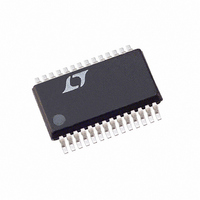
LTC1703CG#TRPBF Linear Technology, LTC1703CG#TRPBF Datasheet - Page 6

LTC1703CG#TRPBF
Manufacturer Part Number
LTC1703CG#TRPBF
Description
IC REG SW DUAL SYNC VID 28SSOP
Manufacturer
Linear Technology
Datasheet
1.LTC1703CG.pdf
(36 pages)
Specifications of LTC1703CG#TRPBF
Applications
Controller, Mobile Intel Pentium® III
Voltage - Input
3 ~ 7 V
Number Of Outputs
2
Voltage - Output
0.9 ~ 2 V
Operating Temperature
0°C ~ 85°C
Mounting Type
Surface Mount
Package / Case
28-SSOP
Lead Free Status / RoHS Status
Lead free / RoHS Compliant
Available stocks
Company
Part Number
Manufacturer
Quantity
Price
LTC1703
PI FU CTIO S
VID n pin includes an on-chip 40kΩ pull-up resistor in
series with a diode (see Block Diagram).
V
except the output drivers are powered from this pin. V
should be connected to a low noise power supply voltage
between 3V and 7V and should be bypassed to SGND with
at least a 1µF capacitor in close proximity to the LTC1703.
FB2 (Pin 19): Controller 2 Feedback Input. FB2 should be
connected through a resistor divider network to V
set the ouput voltage. The loop compensation network for
controller 2 also connects to FB2.
COMP2 (Pin 20): Controller 2 Loop Compensation. See
COMP1.
RUN/SS2 (Pin 21): Controller 2 Run/Soft-Start. See RUN/
SS1.
FAULT (Pin 22): Output Overvoltage Fault (Latched). The
FAULT pin is an open-drain output with an internal 10µA
pull-up. If either regulated output voltage rises more than
15% above its programmed value for more than 25µs, the
FAULT output will go high and the entire LTC1703 will be
TEST CIRCUIT
6
CC
U
(Pin 18): Power Supply Input. All internal circuits
U
MEASURED
f
OSC
V
FB1
U
2000pF
2k
0.1µF
2000pF
NC
NC
I
BOOST1
OUT2
BOOST1
TG1
BG1
SW1
I
FCB
VID0:4
RUN/SS1
COMP1
FB1
SENSE
MAX1
Test Circuit 1
V
GND
CC
CC
to
I
CC
LTC1703
PGND
PV
disabled. When FAULT is high, both BG pins will go high,
turning on the bottom MOSFET switches and pulling down
the high output voltage. The LTC1703 will remain latched
in this state until the power is cycled. When FAULT mode
is active, the FAULT pin will be pulled up with an internal
10µA current source. Tying FAULT directly to SGND will
disable latched FAULT mode and will allow the LTC1703 to
resume normal operation when the overvoltage fault is
removed.
PGND (Pin 23): Power Ground. The BG n drivers return to
this pin. Connect PGND to a high current ground node in
close proximity to the sources of external MOSFETs, QB1
and QB2, and the V
SW2 (Pin 24): Controller 2 Switching Node. See SW1.
TG2 (Pin 25): Controller 2 Top Gate Drive. See TG1.
BG2 (Pin 26): Controller 2 Bottom Gate Drive. See BG1.
BOOST2 (Pin 27): Controller 2 Top Gate Driver Supply.
See BOOST1.
I
5V
RUN/SS2
MAX2
BOOST2
COMP2
CC
FAULT
I
I
PVCC
MAX2
SW2
BG2
TG2
FB2
(Pin 28): Controller 2 Current Limit Set. See I
NC
I
BOOST2
2000pF
2k
+
IN
100µF
and V
2000pF
OUT
bypass capacitors.
V
V
FAULT
FB2
1703 TC
MAX1
1703fa
.


