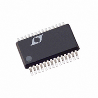
LTC1703CG#TRPBF Linear Technology, LTC1703CG#TRPBF Datasheet - Page 12

LTC1703CG#TRPBF
Manufacturer Part Number
LTC1703CG#TRPBF
Description
IC REG SW DUAL SYNC VID 28SSOP
Manufacturer
Linear Technology
Datasheet
1.LTC1703CG.pdf
(36 pages)
Specifications of LTC1703CG#TRPBF
Applications
Controller, Mobile Intel Pentium® III
Voltage - Input
3 ~ 7 V
Number Of Outputs
2
Voltage - Output
0.9 ~ 2 V
Operating Temperature
0°C ~ 85°C
Mounting Type
Surface Mount
Package / Case
28-SSOP
Lead Free Status / RoHS Status
Lead free / RoHS Compliant
Available stocks
Company
Part Number
Manufacturer
Quantity
Price
APPLICATIO S I FOR ATIO
LTC1703
current limits or QB dies trying to save the load. This
behavior provides maximum protection against overvolt-
age faults at the output, while allowing the circuit to re-
sume normal operation when the fault is removed. The
overvoltage protection circuit can optionally be set to latch
the output off permanently (see the Overvoltage Fault
section).
The MIN comparator (see Block Diagram) trips whenever
FB is more than 5% below 800mV and immediately forces
the switch duty cycle to 90% to bring the output voltage
back into range. It releases when FB is within the 5%
window. MIN is disabled when the soft-start or current
limit circuits are active—the only two times that the
output should legitimately be below its regulated value.
Notice that the FB pin is the virtual ground node of the
feedback amplifier. A typical compensation network does
not include local DC feedback around the amplifier, so that
the DC level at FB will be an accurate replica of the output
voltage, divided down by R1 and R
the compensation capacitors will tend to attenuate AC
signals at FB, especially with low bandwidth type 1 feed-
back loops. This creates a situation where the MIN and
MAX comparators do not respond immediately to shifts in
the output voltage, since they monitor the output at FB.
12
V
RUN/SS
U
V
OUT
0V
5V
0V
U
LTC1703 ENABLED
RUN/SS CONTROLS
DUTY CYCLE
0.5V
1.0V
Figure 4. Soft-Start Operation in Start-Up and Current Limit
START-UP
B
W
(Figure 3). However,
2.5V
COMP CONTROLS DUTY CYCLE
U
4.5V
MIN COMPARATOR ENABLED
NORMAL OPERATION
Maximizing feedback loop bandwidth will minimize these
delays and allow MIN and MAX to operate properly. See
the Feedback Loop/Compensation section.
SHUTDOWN/SOFT-START
Each half of the LTC1703 has a RUN/SS pin. The RUN/SS
pins perform two functions: when pulled to ground, each
shuts down its half of the LTC1703, and each acts as a
conventional soft-start pin, enforcing a maximum duty
cycle limit proportional to the voltage at RUN/SS. An
internal 3.5µA current source pull-up is connected to each
RUN/SS pin, allowing a soft-start ramp to be generated
with a single external capacitor to ground. The 3.5µA
current sources are active even when the LTC1703 is shut
down, ensuring the device will start when any external
pull-down at RUN/SS is released. Either side can be shut
down without affecting the operation of the other side. If
both sides are shut down at the same time, the LTC1703
goes into a micropower sleep mode, and quiescent cur-
rent drops typically below 50µA. Entering sleep mode also
resets the FAULT latch, if it was set.
Each RUN/SS pin shuts down its half of the LTC1703 when
it falls below about 0.5V (Figure 4). Between 0.5V and
about 1V, that half is active, but the maximum duty cycle
CURRENT LIMIT
RUN/SS CONTROLS
2.5V
DUTY CYCLE
1703 F04
1703fa


