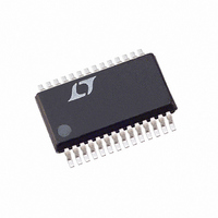
LTC1703CG#TRPBF Linear Technology, LTC1703CG#TRPBF Datasheet - Page 22

LTC1703CG#TRPBF
Manufacturer Part Number
LTC1703CG#TRPBF
Description
IC REG SW DUAL SYNC VID 28SSOP
Manufacturer
Linear Technology
Datasheet
1.LTC1703CG.pdf
(36 pages)
Specifications of LTC1703CG#TRPBF
Applications
Controller, Mobile Intel Pentium® III
Voltage - Input
3 ~ 7 V
Number Of Outputs
2
Voltage - Output
0.9 ~ 2 V
Operating Temperature
0°C ~ 85°C
Mounting Type
Surface Mount
Package / Case
28-SSOP
Lead Free Status / RoHS Status
Lead free / RoHS Compliant
Available stocks
Company
Part Number
Manufacturer
Quantity
Price
APPLICATIO S I FOR ATIO
LTC1703
the LC roll-off happens close to the LC pole, limiting the
total phase shift due to the LC. The additional phase
compensation in the feedback amplifier allows the 0dB
point to be at or above the LC pole frequency, improving
loop bandwidth substantially over a simple type 1 loop. It
has limited ability to compensate for LC combinations
where low capacitor ESR keeps the phase shift near 180°
for an extended frequency range. LTC1703 circuits using
conventional switching grade electrolytic output capaci-
tors can often get acceptable phase margin with type 2
compensation.
“Type 3” loops (Figure 11) use two poles and two zeros to
obtain a 180° phase boost in the middle of the frequency
band. A properly designed type 3 circuit can maintain
acceptable loop stability even when low output capacitor
ESR causes the LC section to approach 180° phase shift
well above the initial LC roll-off. As with a type 2 circuit, the
loop should cross through 0dB in the middle of the phase
bump to maximize phase margin. Many LTC1703 circuits
using low ESR tantalum or OS-CON output capacitors
22
GAIN
(dB)
Figure 10a. Type 2 Amplifier Schematic Diagram
Figure 10b. Type 2 Amplifier Transfer Function
0
IN
GAIN
PHASE
R1
–6dB/OCT
U
R
B
V
REF
U
R2
+
–
C2
–6dB/OCT
C1
W
1703 F10a
OUT
PHASE
0
–90
–180
–270
(DEG)
U
1703 F10b
need type 3 compensation to obtain acceptable phase
margin with a high bandwidth feedback loop.
Feedback Component Selection
Selecting the R and C values for a typical type 2 or type 3
loop is a nontrivial task. The applications shown in this data
sheet show typical values, optimized for the power com-
ponents shown. They should give acceptable performance
with similar power components, but can be way off if even
one major power component is changed significantly.
Applications that require optimized transient response will
need to recalculate the compensation values specifically
for the circuit in question. The underlying mathematics are
complex, but the component values can be calculated in a
straightforward manner if we know the gain and phase of
the modulator at the crossover frequency.
Modulator gain and phase can be measured directly from
a breadboard, or can be simulated if the appropriate
parasitic values are known. Measurement will give more
Figure 11a. Type 3 Amplifier Schematic Diagram
GAIN
(dB)
Figure 11b. Type 3 Amplifier Transfer Function
0
IN
GAIN
PHASE
–6dB/OCT
C3
R1
R
B
R3
+6dB/OCT
V
REF
R2
–
+
C2
C1
–6dB/OCT
1703 F11a
OUT
PHASE
0
–90
–180
–270
1703 F11b
(DEG)
1703fa


