ISL6539CAZ-T Intersil, ISL6539CAZ-T Datasheet - Page 18
ISL6539CAZ-T
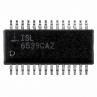
Manufacturer Part Number
ISL6539CAZ-T
Description
IC CTRLR DDR DRAM, SDRAM 28QSOP
Manufacturer
Intersil
Datasheet
1.ISL6539CAZ.pdf
(20 pages)
Specifications of ISL6539CAZ-T
Applications
Controller, DDR DRAM, SDRAM
Voltage - Input
3.3 ~ 18 V
Number Of Outputs
2
Voltage - Output
0.9 ~ 5.5 V
Operating Temperature
0°C ~ 70°C
Mounting Type
Surface Mount
Package / Case
28-QSOP
Lead Free Status / RoHS Status
Lead free / RoHS Compliant
Available stocks
Company
Part Number
Manufacturer
Quantity
Price

Part Number:
ISL6539CAZ-T
Manufacturer:
INTERSIL
Quantity:
20 000


It is a good engineering practice to separate the power
voltage and current flowing path from the control and logic
level signal path. The controller IC will stay on the signal
layer, which is isolated by the signal ground to the power
signal traces.
Component Placement
The control pins of the two-channel ISL6539 are located
symmetrically on two sides of the IC; it is desirable to
arrange the two channels symmetrically around the IC.
The power MOSFET should be close to the IC so that the
gate drive signal, the LAGTEx, UGATEx, PHASEx, BOOTx,
and ISENx traces can be short.
Place the components in such a way that the area under the
ISL6539 has fewer noise traces with high dv/dt and di/dt,
such as gate signals and phase node signals.
Signal Ground and Power Ground Connection
At minimum, a reasonably large area of copper, which will
shield other noise couplings through the IC, could be used
as signal ground beneath the ISL6539. The best tie-point
between the signal ground and the power ground is at the
negative side of the output capacitor on each channel, where
there is less noise. Noisy traces beneath the ISL6539 are
not recommended.
GND and VCC Pins
At least one high quality ceramic decoupling cap should be
used across these two pins. A via can tie GND to signal
ground. Since Pin 1 (GND) and Pin 28 (VCC) are close
together, the decoupling cap can be put close to the IC.
Pin 2 and Pin 27, the LGATE1 and LGATE2
These are the gate drive signals for the bottom MOSFETs of
the buck converter. The signal going through these traces
have both high dv/dt and high di/dt, with high peak charging
and discharging current. These two traces should be short,
wide, and away from other traces. There should be no other
weak signal traces in parallel with these traces on any layer.
Pin 3 and Pin 26, PGND1 and PGND2
Each pin should be laid out to the negative side of the
relevant output cap with separate traces. The negative side
of the output capacitor must be close to the source node of
the bottom MOSFET. These traces are the return path of
LGATE1 and LGATE2.
Pin 4 and Pin 25, the PHASE Pin
These traces should be short, and positioned away from
other weak signal traces. The phase node has a very high
dv/dt with a voltage swing from the input voltage to ground.
No trace should be in parallel with these traces. These
traces are also the return path for UGATE1 and UGATE2.
3. Power Layers: Power Ground
4. Bottom Layer: Power MOSFET, Inductors and other
Power traces
18
ISL6539
Connect these pins to the respective converters’ upper
MOSFET source.
Pin 5 and Pin 24, the UGATE1 and UGATE2
These pins have a square shape waveform with high dv/dt. It
provides the gate drive current to charge and discharge the
top MOSFET with high di/dt. This trace should be wide,
short, and away from other traces similar to the LGATEx.
Pin 6 and Pin 23, the BOOT1 and BOOT2
These pins di/dt are as high as that of the UGATEx;
therefore, the traces should be as short as possible.
Pin 7 and Pin 22, the ISEN1 and ISEN2
The ISEN trace should be a separate trace, and
independently go to the drain terminal of the lower MOSFET.
The current sense resistor should be close to ISEN pin.
The loop formed by the bottom MOSFET, output inductor,
and output capacitor, should be very small. The source of
the bottom MOSFET should tie to the negative side of the
output capacitor in order for the current sense pin to get the
voltage drop on the r
Pin 8 and Pin 21, the EN1 and EN2
These pins stay high in enable mode and low in idle mode
and are relatively robust. Enable signals should refer to the
signal ground.
Pin 10 and Pin 19, VSEN1 and VSEN2
There is usually a resistor divider connecting the output
voltage to this pin. The input impedance of these two pins is
high because they are the input to the amplifiers. The correct
layout should bring the output voltage from the regulation
point to the SEN pin with kelvin traces. Build the resistor
divider close to the pin so that the high impedance trace is
shorter.
Pin 11 and Pin 18, the OCSET1 and OCSET2
In dual switcher mode operation, the overcurrent set resistor
should be put close to this pin. In DDR mode operation, the
voltage divider, which divides the VDQQ voltage in half,
should be put very close to this pin. The other side of the OC
set resistor should connect to signal ground.
Pin 12 and Pin 17, SOFT1 and SOFT2
The soft-start capacitors should be laid out close to this pin.
The other side of the soft-start cap should tie to signal
ground.
Pin 15 and Pin 16, PG1 and PG2 for Dual Switcher
Operation
For dual switcher operations, these two lines are less noise
sensitive. For DDR applications, a capacitor should be
placed to the PG2/REF pin.
Pin 13, DDR
This pin should connect to VCC in DDR applications, and to
signal ground in dual switcher applications.
DS(ON)
.
April 29, 2010
FN9144.6
Related parts for ISL6539CAZ-T
Image
Part Number
Description
Manufacturer
Datasheet
Request
R

Part Number:
Description:
Wide Input Range Dual PWM Controller with DDR Option
Manufacturer:
Intersil Corporation
Datasheet:

Part Number:
Description:
ISL6539 EVAL BOARD 2 - SSOP - Dual Switching Regulator
Manufacturer:
Intersil
Part Number:
Description:
Intersil Corporation [CMOS Serial Controller Interface]
Manufacturer:
Intersil Corporation
Datasheet:
Part Number:
Description:
Manufacturer:
Intersil Corporation
Datasheet:
Part Number:
Description:
357-036-542-201 CARDEDGE 36POS DL .156 BLK LOPRO
Manufacturer:
Intersil Corporation
Datasheet:
Part Number:
Description:
1024-Word x 4-Bit LSI Static RAM
Manufacturer:
Intersil Corporation
Datasheet:
Part Number:
Description:
General Purpose NPN Transistor Arrays FN341.4
Manufacturer:
Intersil Corporation
Datasheet:
Part Number:
Description:
CMOS 16-Bit Microprocessor
Manufacturer:
Intersil Corporation
Datasheet:
Part Number:
Description:
Manufacturer:
Intersil Corporation
Datasheet:
Part Number:
Description:
Manufacturer:
Intersil Corporation
Datasheet:
Part Number:
Description:
Manufacturer:
Intersil Corporation
Datasheet:
Part Number:
Description:
Manufacturer:
Intersil Corporation
Datasheet:
Part Number:
Description:
CMOS 6-Bit Latch and Decoder Memory Interfaces
Manufacturer:
Intersil Corporation
Datasheet:
Part Number:
Description:
CA3046General Purpose NPN Transistor Arrays
Manufacturer:
Intersil Corporation
Datasheet: