ISL6265HRTZ-T Intersil, ISL6265HRTZ-T Datasheet - Page 9
ISL6265HRTZ-T
Manufacturer Part Number
ISL6265HRTZ-T
Description
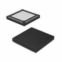
IC CTLR MULTI-OUTPUT 48-TQFN
Manufacturer
Intersil
Datasheet
1.ISL6265HRTZ.pdf
(24 pages)
Specifications of ISL6265HRTZ-T
Applications
Controller, AMD SVI Capable Mobile
Voltage - Input
5 ~ 24 V
Number Of Outputs
3
Voltage - Output
0.5 ~ 1.55 V
Operating Temperature
-10°C ~ 100°C
Mounting Type
Surface Mount
Package / Case
48-TQFN
Lead Free Status / RoHS Status
Lead free / RoHS Compliant


Functional Pin Description
OFS/VFIXEN
VCC
The bias supply for the IC’s control circuitry. Connect this pin
to a +5V supply and decouple using a quality 0.1µF ceramic
capacitor.
VIN
Battery supply voltage. It is used for input voltage feed-forward
to improve the input line transient performance.
PVCC
The power supply pin for the internal MOSFET gate drivers
of the ISL6265. Connect this pin to a +5V power supply.
Decouple this pin with a quality 1.0µF ceramic capacitor.
GND
The bias and reference ground for the IC. The GND
connection for the ISL6265 is through the thermal pad on the
bottom of the package.
RBIAS
A 117kΩ resistor from RBIAS to GND sets internal reference
currents. The addition of capacitance to this pin must be
avoided and can create instabilities in operation.
OFS/VFIXEN
A resistor from this pin to GND programs a DC current
source, which generates a positive offset voltage across the
resistor between FB and VDIFF pins. In this case, the OFS
pin voltage is +1.2V and VFIX mode is not enabled. If OFS is
pulled up to +3.3V, VFIX mode is enabled, the DAC decodes
the SVC and SVD inputs to determine the programmed
voltage, and the OFS function is disabled. If OFS is pulled up
to +5V, the OFS function and VFIX mode are disabled.
COMP_0
ENABLE
VDIFF_0
PWROK
PGOOD
OCSET
RBIAS
FB_0
VW0
SVD
SVC
10
12
11
1
2
3
4
5
6
7
8
9
48
13
47
14
46
15
45
16
44
17
43
18
GND
9
49
42
19
41
20
40
21
39
22
38
23
37
24
36
35
34
33
32
31
30
29
28
27
26
25
BOOT_NB
BOOT_0
UGATE_0
PHASE_0
PGND_0
LGATE_0
PVCC
LGATE_1
PGND_1
PHASE_1
UGATE_1
BOOT_1
ISL6265
PWROK
System power good input. When this pin is high, the SVI
interface is active and I
is low, the SVC, SVD, and VFIXEN input states determine
the pre-PWROK metal VID or VFIX mode voltage. This pin
must be low prior to the ISL6265 PGOOD output going high
per the AMD SVI Controller Guidelines.
PGOOD
Controller power-good open-drain output. This pin is
typically pulled up externally by a 2.0kΩ resistor to +3.3V.
During normal operation, this pin indicates whether all output
voltages are within specified overvoltage and undervoltage
limits and no overcurrent condition is present. If any output
voltage exceeds these limits or a reset event occurs, the pin
is pulled low. This pin is always low prior to the end of
soft-start.
SVC
This pin is the serial VID clock input from the AMD
processor.
SVD
This pin is the serial VID data bidirectional signal to and from
the master device on the AMD processor.
ENABLE
Digital input enable. A high level logic signal on this pin
enables the ISL6265.
FSET_NB
A resistor from this pin to GND programs the switching
frequency of the Northbridge controller (for example,
22.1k ~ 260kHz).
FB_NB
This pin is the output voltage feedback to the inverting input
of the Northbridge controller error amplifier.
COMP_NB
This pin is the output of the Northbridge controller error
amplifier.
VSEN_NB, RTN_NB
Remote Northbridge voltage sense input and return.
Connect isolated traces from these pins to the Northbridge
sense points of the processor.
OCSET_NB
Overcurrent protection selection input for the Northbridge
controller. A resistor from this pin to PHASE_NB sets the OC
trip point.
UGATE_NB
Upper MOSFET gate signal from Northbridge controller.
LGATE_NB
Lower MOSFET gate signal from Northbridge controller.
2
C protocol is running. While this pin
May 13, 2009
FN6599.1
Related parts for ISL6265HRTZ-T
Image
Part Number
Description
Manufacturer
Datasheet
Request
R

Part Number:
Description:
Multi-Output Controller
Manufacturer:
Intersil Corporation
Datasheet:
Part Number:
Description:
Intersil Corporation [CMOS Serial Controller Interface]
Manufacturer:
Intersil Corporation
Datasheet:
Part Number:
Description:
Manufacturer:
Intersil Corporation
Datasheet:
Part Number:
Description:
357-036-542-201 CARDEDGE 36POS DL .156 BLK LOPRO
Manufacturer:
Intersil Corporation
Datasheet:
Part Number:
Description:
1024-Word x 4-Bit LSI Static RAM
Manufacturer:
Intersil Corporation
Datasheet:
Part Number:
Description:
General Purpose NPN Transistor Arrays FN341.4
Manufacturer:
Intersil Corporation
Datasheet:
Part Number:
Description:
CMOS 16-Bit Microprocessor
Manufacturer:
Intersil Corporation
Datasheet:
Part Number:
Description:
Manufacturer:
Intersil Corporation
Datasheet:
Part Number:
Description:
Manufacturer:
Intersil Corporation
Datasheet:
Part Number:
Description:
Manufacturer:
Intersil Corporation
Datasheet:
Part Number:
Description:
Manufacturer:
Intersil Corporation
Datasheet:
Part Number:
Description:
CMOS 6-Bit Latch and Decoder Memory Interfaces
Manufacturer:
Intersil Corporation
Datasheet:
Part Number:
Description:
CA3046General Purpose NPN Transistor Arrays
Manufacturer:
Intersil Corporation
Datasheet:
Part Number:
Description:
Manufacturer:
Intersil Corporation
Datasheet:
Part Number:
Description:
TR909 DLC/FLC SLIC with Low Power Standby
Manufacturer:
Intersil Corporation
Datasheet: