EL5525IREZ-T7 Intersil, EL5525IREZ-T7 Datasheet - Page 2
EL5525IREZ-T7
Manufacturer Part Number
EL5525IREZ-T7
Description
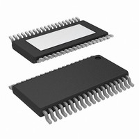
IC VREF GEN 18CH TFTLCD 38HTSSOP
Manufacturer
Intersil
Datasheet
1.EL5525IREZ.pdf
(10 pages)
Specifications of EL5525IREZ-T7
Applications
Converter, TFT, LCD
Voltage - Input
4.5 ~ 16.5 V
Number Of Outputs
18
Voltage - Output
0.5 ~ 14.95 V
Operating Temperature
-40°C ~ 85°C
Mounting Type
Surface Mount
Package / Case
38-TSSOP Exposed Pad, 38-eTSSOP, 38-HTSSOP
Lead Free Status / RoHS Status
Lead free / RoHS Compliant


Absolute Maximum Ratings
Supply Voltage
Maximum Continuous Output Current . . . . . . . . . . . . . . . . . . . 30mA
CAUTION: Do not operate at or near the maximum ratings listed for extended periods of time. Exposure to such conditions may adversely impact product reliability and
result in failures not covered by warranty.
IMPORTANT NOTE: All parameters having Min/Max specifications are guaranteed. Typ values are for information purposes only. Unless otherwise noted, all tests are
at the specified temperature and are pulsed tests, therefore: T
Electrical Specifications
SUPPLY
I
I
ANALOG
V
V
I
PSRR
t
V
ΔV
V
R
REG
BG
DIGITAL
V
V
F
t
t
t
t
t
R
T
Duty Cycle
F_OSC
INL
DNL
S
SD
SC
D
S
H
LC
CE
DCO
PARAMETER
Between V
Between V
AC
CLK
PULSE
OL
OH
DROOP
INH
IH
IL
SDIN
MIS
S
SD
and GND . . . . . . . . . . . . . . . . 4.5V(min) to 18V(max)
and GND . . . . . . . . . . . 3V(min) to V
Supply Current
Digital Supply Current
Output Swing Low
Output Swing High
Short Circuit Current
Power Supply Rejection Ratio
Program to Out Delay
Accuracy Referred to the Ideal Value
Channel to Channel Mismatch
Droop Voltage
Input Resistance @ V
Load Regulation
Band Gap
Logic 1 Input Voltage
Logic 0 Input Voltage
Clock Frequency
Setup Time
Hold Time
Load to Clock Time
Clock to Load Line
Clock to Out Delay Time
S
Minimum Pulse Width for EXT_OSC
Signal
Duty Cycle for EXT_OSC Signal
Internal Refresh Oscillator Frequency
Integral Nonlinearity Error
Differential Nonlinearity Error
DIN
Input Resistance
DESCRIPTION
2
V
otherwise specified.
S
(T
= 15V, V
A
REFH
= +25°C)
, V
SD
REFL
= 5V, V
S
J
and +7(max)
= T
REFH
C
= T
No load
Sinking 5mA (V
Sourcing 5mA (V
R
V
Code = 512
Code = 512
I
Negative edge of SCLK
OSC_Select = 0
OUT
S
L
A
+ is moved from 14V to 16V
= 13V, V
= 10Ω
= 5mA step
EL5525
REFL
CONDITIONS
REFH
Thermal Information
Maximum Die Temperature . . . . . . . . . . . . . . . . . . . . . . . . . . +125°C
Storage Temperature . . . . . . . . . . . . . . . . . . . . . . . .-65°C to +150°C
Pb-Free Reflow Profile. . . . . . . . . . . . . . . . . . . . . . . . .see link below
Operating Conditions
Ambient Operating Temperature . . . . . . . . . . . . . . . .-40°C to +85°C
REFH
= 2V, R
http://www.intersil.com/pbfree/Pb-FreeReflow.asp
= 15V, V
= 15V, V
L
= 1.5kΩ and C
REFL
REFL
= 0)
= 0)
L
= 200pF to 0V, T
14.85
MIN
100
1.1
45
2
14.95
TYP
0.17
140
0.5
1.3
1.3
0.5
15
50
60
20
34
20
20
20
20
10
50
21
A
4
2
1
1
5
= +25°C, unless
MAX
0.35
150
1.5
1.6
18
September 21, 2010
2
1
5
mV/mA
mV/ms
FN7393.2
UNIT
MHz
LSB
LSB
kHz
mA
mA
mV
mA
mV
mV
GΩ
ms
kΩ
dB
ns
ns
ns
ns
ns
µs
%
V
V
V
V
Related parts for EL5525IREZ-T7
Image
Part Number
Description
Manufacturer
Datasheet
Request
R

Part Number:
Description:
Intersil Corporation [CMOS Serial Controller Interface]
Manufacturer:
Intersil Corporation
Datasheet:
Part Number:
Description:
Manufacturer:
Intersil Corporation
Datasheet:
Part Number:
Description:
357-036-542-201 CARDEDGE 36POS DL .156 BLK LOPRO
Manufacturer:
Intersil Corporation
Datasheet:
Part Number:
Description:
1024-Word x 4-Bit LSI Static RAM
Manufacturer:
Intersil Corporation
Datasheet:
Part Number:
Description:
General Purpose NPN Transistor Arrays FN341.4
Manufacturer:
Intersil Corporation
Datasheet:
Part Number:
Description:
CMOS 16-Bit Microprocessor
Manufacturer:
Intersil Corporation
Datasheet:
Part Number:
Description:
Manufacturer:
Intersil Corporation
Datasheet:
Part Number:
Description:
Manufacturer:
Intersil Corporation
Datasheet:
Part Number:
Description:
Manufacturer:
Intersil Corporation
Datasheet:
Part Number:
Description:
Manufacturer:
Intersil Corporation
Datasheet:
Part Number:
Description:
CMOS 6-Bit Latch and Decoder Memory Interfaces
Manufacturer:
Intersil Corporation
Datasheet:
Part Number:
Description:
CA3046General Purpose NPN Transistor Arrays
Manufacturer:
Intersil Corporation
Datasheet:
Part Number:
Description:
Manufacturer:
Intersil Corporation
Datasheet:
Part Number:
Description:
TR909 DLC/FLC SLIC with Low Power Standby
Manufacturer:
Intersil Corporation
Datasheet:
Part Number:
Description:
Manufacturer:
Intersil Corporation
Datasheet: