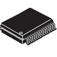
MCZ34702EWR2 Freescale Semiconductor, MCZ34702EWR2 Datasheet - Page 16

MCZ34702EWR2
Manufacturer Part Number
MCZ34702EWR2
Description
IC PWR SUPPLY 3A SW 32-SOIC
Manufacturer
Freescale Semiconductor
Datasheet
1.MC34702EK.pdf
(39 pages)
Specifications of MCZ34702EWR2
Applications
Controller, Power QUICC™ I, II
Voltage - Input
2.8 ~ 6 V
Number Of Outputs
2
Voltage - Output
7.75V, 0.8 ~ 6 V
Operating Temperature
-40°C ~ 85°C
Mounting Type
Surface Mount
Package / Case
32-SOIC (7.5mm Width)
Output Current
3 A
Input Voltage
2.8 V to 6 V
Switching Frequency
300 KHz
Mounting Style
SMD/SMT
Duty Cycle (max)
95 %
Lead Free Status / RoHS Status
Lead free / RoHS Compliant
means to efficiently supply the Freescale Power QUICC and
other families of Freescale microprocessors. It incorporates a
high performance synchronous buck regulator, supplying the
microprocessor’s core, and a low dropout (LDO) linear
regulator providing the microprocessor I/O and bus voltages.
OSCILLATOR FREQUENCY PIN (FREQ)
connecting external resistor RF to the FREQ pin. The default
switching frequency (FREQ pin left open or tied to VDDI) is
set to 300kHz.
INVERTING INPUT PIN (INV)
OUTPUT VOLTAGE PIN (VOUT)
switching regulator power sequence control circuit.
INPUT VOLTAGE 2 PINS (VIN2)
MOSFET.
SWITCH PINS (SW)
inductor.
GROUND PINS (GND)
POWER GROUND PINS (PGND)
BOOST DRAIN PIN (VBD)
BOOST VOLTAGE PIN (VBST)
regulator provides a 20mA output current to supply the drive
circuits for the integrated power MOSFETs and the external
N-channel power MOSFET of the linear regulator. The
voltage at the VBST pin is 7.75V nominal.
16
34702
FUNCTIONAL DESCRIPTION
INTRODUCTION
The 34702 power supply integrated circuit provides the
This switcher frequency selection pin can be adjusted by
Buck Controller Error Amplifier inverting input.
Output voltage of the buck converter. Input pin of the
Buck regulator power input. Drain of the high side power
Buck regulator switching node. This pin is connected to the
Analog ground of the IC, thermal heatsinking.
Buck regulator power ground.
Drain of the internal boost regulator power MOSFET.
Internal boost regulator output voltage. The internal boost
FUNCTIONAL DESCRIPTION
FUNCTIONAL PIN DESCRIPTION
INTRODUCTION
precisely maintained up/down power sequencing, ensuring
the proper operation and protection of the CPU and power
system. At the same time, it provides high flexibility of
configuration, allowing the maximum optimization of the
power supply system.
BOOTSTRAP PIN (BOOT)
SERIAL DATA PIN (SDA)
SERIAL CLOCK PIN (SCL)
LINEAR COMPENSATION PIN (LCMP)
LINEAR FEEDBACK PIN (LFB)
LINEAR REGULATOR PIN (LDO)
circuit.
CURRENT SENSE PIN (CS)
the linear regulator external power MOSFET. The voltage
drop over the LDO current sense resistor RS is sensed
between the CS and LDO pins. The LDO current limit can be
adjusted by selecting the proper value of the current sensing
resistor RS.
LINEAR DRIVE PIN (LDRV)
INPUT VOLTAGE 1 PIN (VIN1)
circuits of the IC are supplied through this pin.
This device incorporates many advanced features; e.g.,
Bootstrap capacitor input.
I
I
Linear regulator compensation pin.
Linear regulator feedback pin.
Input pin of the linear regulator power sequence control
Current sense pin of the LDO. Over-current protection of
LDO gate drive of the external pass N-channel MOSFET.
The input supply pin for the integrated circuit. The internal
2
2
C bus pin. Serial data.
C bus pin. Serial clock.
Analog Integrated Circuit Device Data
Freescale Semiconductor


