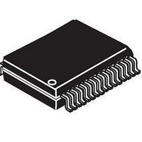
MCZ34702EWR2 Freescale Semiconductor, MCZ34702EWR2 Datasheet - Page 23

MCZ34702EWR2
Manufacturer Part Number
MCZ34702EWR2
Description
IC PWR SUPPLY 3A SW 32-SOIC
Manufacturer
Freescale Semiconductor
Datasheet
1.MC34702EK.pdf
(39 pages)
Specifications of MCZ34702EWR2
Applications
Controller, Power QUICC™ I, II
Voltage - Input
2.8 ~ 6 V
Number Of Outputs
2
Voltage - Output
7.75V, 0.8 ~ 6 V
Operating Temperature
-40°C ~ 85°C
Mounting Type
Surface Mount
Package / Case
32-SOIC (7.5mm Width)
Output Current
3 A
Input Voltage
2.8 V to 6 V
Switching Frequency
300 KHz
Mounting Style
SMD/SMT
Duty Cycle (max)
95 %
Lead Free Status / RoHS Status
Lead free / RoHS Compliant
STANDARD POWER SEQUENCING
Sequencing Mode, the switcher output provides the core
voltage for the microprocessor. This situation and operating
conditions are illustrated in
page 17, shows the Power Sequencing Mode selection.
INVERTED POWER SEQUENCING
Power Sequencing Mode, the linear regulator (LDO) output
provides the core voltage for the microprocessor, as
illustrated in
Sequencing Mode selection.
Analog Integrated Circuit Device Data
Freescale Semiconductor
1.8V Start-Up
∆V = 2.1 V
Max. Lead
When the power supply IC operates in the Standard Power
When the power supply IC is operating in the Inverted
Optional
5.0 V
Figure 18. Standard Power-up / Down Sequence
Figure
3.3 V I/O Voltage (VLDO)
5.0 V Input Supply
ADDR
GND
VIN2
VBD
RT
SDA
SCL
CLKSYN
CLKSEL
FREQ
VBST
EN1
EN2
in +5.0V Supply System
∆V = 0.4 V
Max. Lag
1.5 V Core Voltage
34702
19.
5.0 V Input
BOOT
PGND
Table 5
LDRV
VOUT
VDDI
VIN1
LDO
RST
LFB
SW
INV
CS
Figures 17
shows the Power
∆V = 0.4 V
Max. Lag
VBST
(VOUT)
and 18.
3.3 V
1.5 V
Table
VDDH (I/Os)
VDDL (Core)
∆V = 2.1 V
Max. Lead
MCU
5,
ASSUMED REQUIREMENTS
Methods of Control
controlling the regulator output voltages, as described in the
paragraphs below. Power sequencing control is also
achieved through the intrinsic operation of the regulators.
The EN1 and EN2 pins can be used to select the proper
Power Sequencing Mode required by the powered system or
to disable the power sequencing (refer to
Intrinsic Operation
voltage is below the regulation point, the LDO external Pass
MOSFET is on, or the buck high side MOSFET is on at a duty
cycle controlled by the switcher. Because these devices are
MOSFETs, current can flow in either direction, balancing the
voltages via the common supply pin. The ability to maintain
the MOSFETs on is dependent on the available gate voltage,
and thus the size of the boost regulator storage capacitor.
1.8V Start-Up
Figure 19. Inverted Power-up / Down Sequence in +5.0V
∆V = 2.1 V
Max. Lead
1. I/O supply voltage not to exceed core voltage by more
2. Core supply voltage not to exceed I/O voltage by more
Optional
The 34702 has several methods of monitoring and
For both the LDO and switcher, whenever the output
5.0 V
than 2.0V.
than 0.4V.
3.3 V I/O Voltage (VOUT)
5.0 V Input Supply
1.5 V Core Voltage (VLDO)
ADDR
GND
SDA
VIN2
VBD
VBST
RT
SCL
EN1
EN2
CLKSYN
CLKSEL
FREQ
∆V = 0.4 V
Max. Lag
34702
5.0 V Input
Supply System
BOOT
PGND
VOUT
LDRV
VDDI
VIN1
LDO
RST
LFB
SW
INV
CS
FUNCTIONAL DEVICE OPERATION
∆V = 0.4 V
Max. Lag
VBST
OPERATIONAL MODES
Table
1.5 V
3.3 V
VDDL (Core)
5).
VDDH (I/Os)
∆V = 2.1 V
Max. Lead
MCU
34702
23


