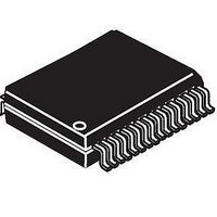
MCZ34702EWR2 Freescale Semiconductor, MCZ34702EWR2 Datasheet - Page 18

MCZ34702EWR2
Manufacturer Part Number
MCZ34702EWR2
Description
IC PWR SUPPLY 3A SW 32-SOIC
Manufacturer
Freescale Semiconductor
Datasheet
1.MC34702EK.pdf
(39 pages)
Specifications of MCZ34702EWR2
Applications
Controller, Power QUICC™ I, II
Voltage - Input
2.8 ~ 6 V
Number Of Outputs
2
Voltage - Output
7.75V, 0.8 ~ 6 V
Operating Temperature
-40°C ~ 85°C
Mounting Type
Surface Mount
Package / Case
32-SOIC (7.5mm Width)
Output Current
3 A
Input Voltage
2.8 V to 6 V
Switching Frequency
300 KHz
Mounting Style
SMD/SMT
Duty Cycle (max)
95 %
Lead Free Status / RoHS Status
Lead free / RoHS Compliant
INTRODUCTION
buck regulator, supplying the microprocessor’s core, and a
low dropout (LDO) linear regulator providing the
microprocessor I / O and bus voltages. This device
BOOST REGULATOR
properly drive the buck regulator power MOSFETs,
especially during the low input voltage condition. The LDO
regulator external N-channel MOSFET gate is also powered
from the boost regulator. In order to properly enhance the
high side MOSFETs when only a +3.3V supply rail powers
the integrated circuit, the boost regulator provides an output
voltage of 7.75V nominal value.
current control technique, which allows fast power-up and
does not require any compensation. When the boost
regulator main power switch (low side) is turned on, the
current in the inductor starts to ramp up. After the inductor
current reaches the upper current limit (nominally set at
1.0A), the low side switch is turned off and the current
charges the output capacitor through the internal rectifier.
18
34702
FUNCTIONAL DESCRIPTION
FUNCTIONAL INTERNAL BLOCK DESCRIPTION
The 34702 incorporates a high-performance synchronous
A boost regulator provides a high voltage necessary to
The 34702 boost regulator uses a simple hysteretic
Buck Control Logic
Boost Regulator
Buck HS and
LS Driver
Switcher
Oscillator
300 kHz
FUNCTIONAL INTERNAL BLOCK DESCRIPTION
Figure 11. 34702 Functional Internal Block Diagram
Power Sequencing
Voltage Margining
Linear Regulator
Watchdog Timer
I
2
C Interface
Control
Internal
Supply
VDDI
I
LIM
incorporates many advanced features; e.g., precisely
maintained up / down power sequencing, ensuring the proper
operation and protection of the CPU and power system.
When the inductor current falls below the valley current limit
value (nominally 600mA), the low side switch is turned on
again, starting the next switching cycle. After the boost
regulator output capacitor reaches approximately 6.0 volts,
the peak and valley current limit levels are proportionally
scaled down to approximately one fifth of their original values.
When the boost regulator reaches its regulation limit (7.75V
typical), the low side switch is turned off until the output
voltage falls below the regulation limit again.
boost regulator start-up sequence allow fast power-up of the
whole IC, while the normal operation with reduced current
limit greatly reduces the switching noise and therefore
improves the overall EMC performance. See
the boost regulator output voltage and inductor current
waveforms (picture not to scale).
The higher current limit values in the beginning of the
Thermal Shutdown
Reset Control
POR Timer
Reference
Reference
Bandgap
Analog Integrated Circuit Device Data
Bandgap
Voltage
Voltage
UVLO
Freescale Semiconductor
Figure 12
for


