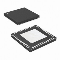
ISL6333CRZ Intersil, ISL6333CRZ Datasheet - Page 27

ISL6333CRZ
Manufacturer Part Number
ISL6333CRZ
Description
IC CTRLR PWM 3PHASE BUCK 48-QFN
Manufacturer
Intersil
Datasheet
1.ISL6333ACRZ.pdf
(40 pages)
Specifications of ISL6333CRZ
Applications
Controller, Intel VR11
Voltage - Input
5 ~ 12 V
Number Of Outputs
1
Voltage - Output
0.5 ~ 1.6 V
Operating Temperature
0°C ~ 70°C
Mounting Type
Surface Mount
Package / Case
48-VQFN
Lead Free Status / RoHS Status
Lead free / RoHS Compliant
Available stocks
Company
Part Number
Manufacturer
Quantity
Price
Part Number:
ISL6333CRZ-T
Manufacturer:
INTERSIL
Quantity:
20 000
.
Gate Voltage Optimization Technology (GVOT)
(ISL6333, ISL6333B Only)
The ISL6333 and ISL6333B are designed to optimize the
Channel 1 lower MOSFET gate drive voltage to ensure high
efficiency in both normal and low power states. In the normal
power state when the converter load current is high, the
conduction losses of the lower MOSFETs play a large role in
the overall system efficiency. In normal power state, the
lower gate drive voltage should be higher to decrease the
conduction losses of the lower MOSFETs and increase the
system efficiency. In the low power state, where the
converter load current is significantly smaller, MOSFET
driving loss becomes a much higher percentage of power
loss associated with the lower MOSFET. In low power state,
the lower gate drive voltage can therefore be reduced to
decrease the driving losses of the lower MOSFETs and
increase the system efficiency.
This gate drive voltage optimization is accomplished by an
internal linear regulator that regulates the Channel 1 lower
gate drive voltage, LVCC1, to certain levels depending on
the state of the PSI# and SS pins. The input and output of
this internal regulator is the PVCC1 pin and BYP1 pin,
respectively. The regulator input, PVCC1, should be
connected to a +12V source and decoupled with a quality
1.0µF ceramic capacitor. The regulator output, BYP1, is
internally connected to the lower gate drive of the Channel 1
MOSFET driver, LVCC1. The BYP1 pin should also be
decoupled using a quality 1.0µF ceramic capacitor.
+5V TO
FIGURE 12. INTERNAL GATE DRIVE CONNECTIONS AND
EXTERNAL CIRCUIT
+12V
+12V
+12V
1.0µF
1.0µF
1.0µ
1.0µ
GAVE VOLTAGE OPTIMIZATION (GVOT)
PVCC2_3
F
F
PUVCC
PVCC1
BYP1
ISL6333, ISL6333B INTERNAL CIRCUIT
27
LVCC = LOWER GATE DRIVE
UVCC = UPPER GATE DRIVE
UVCC1, UVCC2,
LVCC2, LVCC3
GVOT
REG.
UVCC3
LVCC1
ISL6333, ISL6333A, ISL6333B, ISL6333C
SET BY STATE
OF PSI# AND
SS PINS
As Figures 13 and 14 illustrate, the internal regulator has
been designed so that its output voltage, BYP1, is dependent
upon the average load current. In the normal power state,
when PSI# is high, the ISL6333 and ISL6333B regulate BYP1
to around 11.2V at a 50mA average load current. In the low
power state, when PSI# is low, BYP1 is regulated down to one
of two voltages depending on the state of the SS pin. If the SS
pin is tied to ground through the R
regulated down to 5.75V at a 50mA average load current. If
the SS pin is tied to VCC through the R
regulated down to 7.75V at a 50mA average load current.
It is possible to disable the internal GVOT regulator by shorting
the PVCC1 pin to the BYP1 pin. This essentially bypasses the
internal regulator setting the Channel 1 lower gate drive
voltage, LVCC1, to the voltage input on the PVCC1 pin.
FIGURE 14. BYP1, LVCC1 VOLTAGE WHEN PSI# IS LOW
FIGURE 13. BYP1, LVCC1 VOLTAGE WHEN PSI# IS HIGH
12.0
11.8
11.6
11.4
11.2
11.0
10.8
10.6
10.4
8.5
8.0
7.5
7.0
6.5
6.0
5.5
5.0
0
0
20
20
AVERAGE LOAD CURRENT (mA)
AVERAGE LOAD CURRENT (mA)
40
40
R
60
60
SS
SS
TIED TO GND
resistor, BYP1 is
SS
R
SS
80
80
resistor, BYP1 is
+40°C THERMAL
TIED TO VCC
+40°C THERMAL
100
100
October 8, 2010
FN6520.3
120
120


