ISL6333AIRZ Intersil, ISL6333AIRZ Datasheet - Page 31

ISL6333AIRZ
Manufacturer Part Number
ISL6333AIRZ
Description
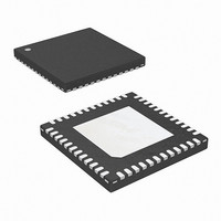
IC CTRLR PWM 3PHASE BUCK 48-QFN
Manufacturer
Intersil
Datasheet
1.ISL6333ACRZ.pdf
(40 pages)
Specifications of ISL6333AIRZ
Applications
Controller, Intel VR11
Voltage - Input
5 ~ 12 V
Number Of Outputs
1
Voltage - Output
0.5 ~ 1.6 V
Operating Temperature
-40°C ~ 85°C
Mounting Type
Surface Mount
Package / Case
48-VQFN
Rohs Compliant
YES
Lead Free Status / RoHS Status
Lead free / RoHS Compliant
Available stocks
Company
Part Number
Manufacturer
Quantity
Price
Company:
Part Number:
ISL6333AIRZ
Manufacturer:
Intersil
Quantity:
215
Individual Channel Overcurrent Limiting
The controllers have the ability to limit the current in each
individual channel without shutting down the entire regulator.
This is accomplished by continuously comparing the sensed
currents of each channel with a constant 140µA OCL
reference current, as shown in Figure 18. If a channel’s
individual sensed current exceeds this OCL limit, the UGATE
signal of that channel is immediately forced low, and the
LGATE signal is forced high. This turns off the upper
MOSFET(s), turns on the lower MOSFET(s), and stops the
rise of current in that channel, forcing the current in the
channel to decrease. That channel’s UGATE signal will not
be able to return high until the sensed channel current falls
back below the 140µA reference.
During VID-on-the-fly transitions the OCL trip level is
boosted to prevent false overcurrent limiting events that can
occur. Starting from the beginning of a dynamic VID
transition, the overcurrent trip level is boosted to 196µA. The
OCL level will stay at this boosted level until 50µs after the
end of the dynamic VID transition, at which point it will return
to the typical 140µA trip level.
MOSFETs General Design Guide
This design guide is intended to provide a high-level
explanation of the steps necessary to create a multi-phase
power converter. It is assumed that the reader is familiar with
many of the basic skills and techniques referenced in the
following. In addition to this guide, Intersil provides complete
reference designs that include schematics, bills of materials,
and example board layouts for all common microprocessor
applications.
Power Stages
The first step in designing a multi-phase converter is to
determine the number of phases. This determination
depends heavily on the cost analysis, which in turn depends
on system constraints that differ from one design to the next.
Principally, the designer will be concerned with whether
components can be mounted on both sides of the circuit
FIGURE 19. OVERCURRENT BEHAVIOR IN HICCUP MODE
0A
0V
OUTPUT CURRENT, 50A/DIV
OUTPUT VOLTAGE,
500mV/DIV
31
ISL6333, ISL6333A, ISL6333B, ISL6333C
board, whether through-hole components are permitted, the
total board space available for power-supply circuitry, and
the maximum amount of load current. Generally speaking,
the most economical solutions are those in which each
phase handles between 25A and 30A. All surface-mount
designs will tend toward the lower end of this current range.
If through-hole MOSFETs and inductors can be used, higher
per-phase currents are possible. In cases where board
space is the limiting constraint, current can be pushed as
high as 40A per phase, but these designs require heat sinks
and forced air to cool the MOSFETs, inductors and
heat-dissipating surfaces.
MOSFETS
The choice of MOSFETs depends on the current each
MOSFET will be required to conduct, the switching frequency,
the capability of the MOSFETs to dissipate heat, and the
availability and nature of heat sinking and air flow.
LOWER MOSFET POWER CALCULATION
The calculation for power loss in the lower MOSFET is
simple, since virtually all of the loss in the lower MOSFET is
due to current conducted through the channel resistance
(r
output current, I
Equation 1), and d is the duty cycle (V
An additional term can be added to the lower-MOSFET loss
equation to account for additional loss accrued during the dead
time when inductor current is flowing through the
lower-MOSFET body diode. This term is dependent on the
diode forward voltage at I
f
and the end of the lower-MOSFET conduction interval
respectively.
The total maximum power dissipated in each lower MOSFET
is approximated by the summation of P
UPPER MOSFET POWER CALCULATION
In addition to r
upper-MOSFET losses are due to currents conducted across
the input voltage (V
higher portion of the upper-MOSFET losses are dependent on
switching frequency, the power calculation is more complex.
Upper MOSFET losses can be divided into separate
components involving the upper-MOSFET switching times,
the lower-MOSFET body-diode reverse-recovery charge, Q
and the upper MOSFET r
P
P
S
LOW 2 ( )
DS(ON)
LOW 1 ( )
, and the length of dead times, t
). In Equation 24, I
=
=
V
r
D ON
DS ON
(
DS(ON)
(
P-P
)
⋅
)
IN
f
is the peak-to-peak inductor current (see
⋅
S
) during switching. Since a substantially
⎛
⎜
⎝
⋅
losses, a large portion of the
I
----- -
N
⎛
⎜
⎝
M
I M
------
M
N
⎞
⎟
⎠
DS(ON)
, V
2
+
M
⋅
I
-----------
(
D(ON)
P-P
1 d
2
is the maximum continuous
–
⎞
⎟
⎠
d1
conduction loss.
⋅
)
, the switching frequency,
t
d1
+
and t
I
--------------------------------------- -
L P-P
+
OUT
(
⎛
⎜
⎜
⎝
LOW(1)
d2
I M
------
N
, at the beginning
)
12
/V
–
2
⋅
I
-----------
(
P-P
IN
1 d
2
).
–
and P
⎞
⎟
⎟
⎠
⋅
October 8, 2010
)
t
d2
(EQ. 25)
LOW(2)
(EQ. 24)
FN6520.3
rr
,
.


