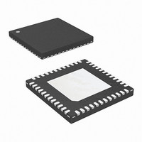
ISL6333AIRZ-T Intersil, ISL6333AIRZ-T Datasheet - Page 19

ISL6333AIRZ-T
Manufacturer Part Number
ISL6333AIRZ-T
Description
IC CTRLR PWM 3PHASE BUCK 48-QFN
Manufacturer
Intersil
Datasheet
1.ISL6333ACRZ.pdf
(40 pages)
Specifications of ISL6333AIRZ-T
Applications
Controller, Intel VR11
Voltage - Input
5 ~ 12 V
Number Of Outputs
1
Voltage - Output
0.5 ~ 1.6 V
Operating Temperature
-40°C ~ 85°C
Mounting Type
Surface Mount
Package / Case
48-VQFN
Lead Free Status / RoHS Status
Lead free / RoHS Compliant
Available stocks
Company
Part Number
Manufacturer
Quantity
Price
upper MOSFET and turns on the lower synchronous
MOSFET. When the modified V
modulator ramp, the PWM output transitions high, turning off
the synchronous MOSFET and turning on the upper
MOSFET. The PWM signal will remain high until the modified
V
occurs the PWM signal will transition low again.
During each PWM time interval, the PWM signal can only
transition high once. Once PWM transitions high it cannot
transition high again until the beginning of the next PWM
time interval. This prevents the occurrence of double PWM
pulses occurring during a single period.
Adaptive Phase Alignment (APA)
To further improve the transient response, the controllers
also implement Intersil’s proprietary Adaptive Phase
Alignment (APA) technique, which turns on all of the
channels together at the same time during large current
step, high di/dt transient events. As Figure 3 shows, the APA
circuitry works by monitoring the voltage on the APA pin and
comparing it to a filtered copy of the voltage on the COMP
pin. The voltage on the APA pin is a copy of the COMP pin
voltage that has been negatively offset. If the APA pin
exceeds the filtered COMP pin voltage an APA event occurs
and all of the channels are forced on.
The APA trip level is the amount of DC offset between the
COMP pin and the APA pin. This is the voltage excursion
that the APA and COMP pin must have during a transient
event to activate the Adaptive Phase Alignment circuitry.
This APA trip level is set through a resistor, R
connects from the APA pin to the COMP pin. A 100µA
current flows across R
trip level as described in Equation 3. An APA trip level of
500mV is recommended for most applications. A 1000pF
capacitor, C
resistor to help with noise immunity.
C
V
COMP
APA
APA TRIP
FIGURE 3. ADAPTIVE PHASE ALIGNMENT DETECTION
(
EXTERNAL CIRCUIT
voltage crosses the modulator ramp again. When this
R
APA
)
APA
=
R
, should also be placed across the R
V
APA
-
APA,TRIP
COMP
APA
⋅
100
APA
×
into the APA pin to set the APA
10
19
ISL6333 INTERNAL CIRCUIT
–
6
COMP
100µA
ISL6333, ISL6333A, ISL6333B, ISL6333C
FILTER
AMPLIFIER
PASS
voltage crosses the
LOW
ERROR
APA
+
-
APA
, that
CIRCUITRY
APA
TO APA
(EQ. 3)
Number of Active Channels
The default number of active channels on the controllers is
three for 3-phase operation. If 2-phase operation is desired,
the ISEN3- pin should be tied to the VCC pin. This will
disable Channel 3, so only Channel 1 and 2 will fire. In
2-phase operation all of the Channel 3 pins should be left
unconnected including the PHASE3, LGATE3, UGATE3,
BOOT3, and ISEN3+ pins.
PSI# (Low Power State) Operation
The controllers are designed to operate in both their normal
power state for high efficiency at heavy loads, and a low
power state to increase the regulator’s light load efficiency.
The power state of the regulator is controlled by the PSI#
pin, which is a digital logic input. When this pin is set HIGH
the regulators will operate in their normal power state, with
all active channels firing in continuous conduction mode
(CCM). When the PSI# pin is set LOW the controllers
change their operating state to the low power state to
increase light load efficiency. The different controllers have
different low power operating states as described in Table 1
and the following sections.
It’s important to note that during soft-start and dynamic VID
transitions the PSI# pin is ignored and the controllers are
forced to run in their normal power state. The state of the
PSI# pin is considered again at the end of a successful
soft-start sequence or dynamic VID transition.
ISL6333, ISL6333B LOW POWER STATE
On the ISL6333 and ISL6333B, when the PSI# pin is set
LOW, the controllers change their operating state in multiple
ways. First, all active channels are turned off accept for
Channel 1. Channel 1 continues to operate but does so in
diode emulation mode (DEM). DEM only allows the upper and
lower MOSFETs to turn on to allow positive current to flow
through the output inductor. If the inductor current falls to 0A
during a switching cycle, both the lower and upper MOSFETs
are turned off to allow no negative current to build up in the
inductor. This helps to decrease the conduction losses of the
MOSFETs and the inductor at very low load currents.
When the ISL6333 and ISL6333B are operating in DEM, it’s
important for the controllers to know whether the output
inductors are standard inductors or coupled inductors. PWM
operation is optimized for use with coupled inductors by
minimizing switching losses and body-diode conduction
CONTROLLER
ISL6333A,
ISL6333B
ISL6333C
ISL6333,
TABLE 1. POWER STATE OPERATION DESCRIPTION
HIGH
HIGH
LOW
LOW
PSI#
3/2-phase
3/2-phase
1-phase
1-phase
COUNT
PHASE
CCM OR
CCM
CCM
CCM
DEM
DEM
October 8, 2010
GVOT
Yes
Yes
No
No
FN6520.3


