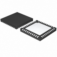
ISL6566CRZ Intersil, ISL6566CRZ Datasheet - Page 9

ISL6566CRZ
Manufacturer Part Number
ISL6566CRZ
Description
IC CTRLR PWM BUCK 3PHASE 40QFN
Manufacturer
Intersil
Datasheet
1.ISL6566CRZ-TR5184.pdf
(29 pages)
Specifications of ISL6566CRZ
Applications
Controller, Intel VRM9, VRM10, and AMD Hammer Applications
Voltage - Input
3 ~ 12 V
Number Of Outputs
1
Voltage - Output
0.84 ~ 1.6 V
Operating Temperature
0°C ~ 70°C
Mounting Type
Surface Mount
Package / Case
40-VFQFN, 40-VFQFPN
Lead Free Status / RoHS Status
Lead free / RoHS Compliant
Available stocks
Company
Part Number
Manufacturer
Quantity
Price
Company:
Part Number:
ISL6566CRZ
Manufacturer:
HARRIS
Quantity:
16 269
Part Number:
ISL6566CRZ
Manufacturer:
INTERSIL
Quantity:
20 000
Company:
Part Number:
ISL6566CRZ-T
Manufacturer:
INTERSIL
Quantity:
3 340
VID4, VID3, VID2, VID1, VID0, and VID12.5
These are the inputs for the internal DAC that provides the
reference voltage for output regulation. These pins respond to
TTL logic thresholds. The ISL6566 decodes the VID inputs to
establish the output voltage; see VID Tables for
correspondence between DAC codes and output voltage
settings. These pins are internally pulled high, to
approximately 1.2V, by 40µA (typically) internal current
sources; the internal pull-up current decreases to 0 as the VID
voltage approaches the internal pull-up voltage. All VID pins
are compatible with external pull-up voltages not exceeding
the IC’s bias voltage (VCC).
VRM10
This pin selects VRM10.0 DAC compliance when pulled high or
open. If VRM10 is grounded, VID12.5 selects the compliance
standard for the internal DAC: pulled to ground, it encodes the
DAC with AMD Hammer VID codes, while left open or pulled
high, it encodes the DAC with Intel VRM9.0 codes.
VSEN and RGND
VSEN and RGND are inputs to the precision differential
remote-sense amplifier and should be connected to the sense
pins of the remote load.
ICOMP, ISUM, and IREF
ISUM, IREF, and ICOMP are the DCR current sense
amplifier’s negative input, positive input, and output
respectively. For accurate DCR current sensing, connect a
resistor from each channel’s phase node to ISUM and
connect IREF to the summing point of the output inductors,
roughly Vout. A parallel R-C feedback circuit connected
between ISUM and ICOMP will then create a voltage from
IREF to ICOMP proportional to the voltage drop across the
inductor DCR. This voltage is referred to as the droop voltage
and is added to the differential remote-sense amplifier output.
Note: An optional 0.01µF ceramic capacitor can be placed
from the IREF pin to the ISUM pin, or from the IREF pin to
GND to help reduce any noise affects that may occur due to
layout.
VDIFF
VDIFF is the output of the differential remote-sense amplifier.
The voltage on this pin is equal to the difference between
VSEN and RGND added to the difference between IREF and
ICOMP. VDIFF therefore represents the output voltage plus
the droop voltage.
FB and COMP
These pins are the internal error amplifier inverting input and
output respectively. FB, VDIFF, and COMP are tied together
through external R-C networks to compensate the regulator.
REF
The REF input pin is the positive input of the error amplifier. It
is internally connected to the DAC output through a 1kΩ
resistor. A capacitor is used between the REF pin and ground
9
ISL6566
ISL6566
to smooth the voltage transition during Dynamic VID
operations.
OFS
The OFS pin provides a means to program a dc current for
generating an offset voltage across the resistor between FB
and VDIFF. The offset current is generated via an external
resistor and precision internal voltage references. The polarity
of the offset is selected by connecting the resistor to GND or
VCC. For no offset, the OFS pin should be left unconnected.
OCSET
This is the overcurrent set pin. Placing a resistor from OCSET
to ICOMP allows a 100µA current to flow out this pin,
producing a voltage reference. Internal circuitry compares the
voltage at OCSET to the voltage at ISUM, and if ISUM ever
exceeds OCSET, the overcurrent protection activates.
ISEN1, ISEN2 and ISEN3
These pins are used for balancing the channel currents by
sensing the current through each channel’s lower MOSFET
when it is conducting. Connect a resistor between the
ISEN1, ISEN2, and ISEN3 pins and their respective phase
node. This resistor sets a current proportional to the current
in the lower MOSFET during its conduction interval.
UGATE1, UGATE2, and UGATE3
Connect these pins to the corresponding upper MOSFET
gates. These pins are used to control the upper MOSFETs
and are monitored for shoot-through prevention purposes.
Maximum individual channel duty cycle is limited to 66%.
BOOT1, BOOT2, and BOOT3
These pins provide the bias voltage for the corresponding
upper MOSFET drives. Connect these pins to appropriately-
chosen external bootstrap capacitors. Internal bootstrap
diodes connected to the PVCC pins provide the necessary
bootstrap charge.
PHASE1, PHASE2, and PHASE3
Connect these pins to the sources of the corresponding
upper MOSFETs. These pins are the return path for the
upper MOSFET drives.
LGATE1, LGATE2, and LGATE3
These pins are used to control the lower MOSFETs. Connect
these pins to the corresponding lower MOSFETs’ gates.
PGOOD
During normal operation PGOOD indicates whether the
output voltage is within specified overvoltage and
undervoltage limits. If the output voltage exceeds these limits
or a reset event occurs (such as an overcurrent event),
PGOOD is pulled low. PGOOD is always low prior to the end
of soft-start.
March 9, 2006
FN9178.4


