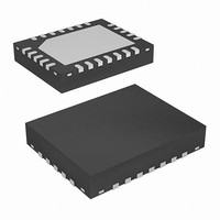
EL5825ILZ-T7 Intersil, EL5825ILZ-T7 Datasheet - Page 9

EL5825ILZ-T7
Manufacturer Part Number
EL5825ILZ-T7
Description
IC VREF GEN 8CH TFT-LCD 24-QFN
Manufacturer
Intersil
Datasheet
1.EL5825IR.pdf
(12 pages)
Specifications of EL5825ILZ-T7
Applications
Converter, TFT, LCD
Voltage - Input
4.5 ~ 16.5 V
Number Of Outputs
8
Voltage - Output
0.5 ~ 14.95 V
Operating Temperature
-40°C ~ 85°C
Mounting Type
Surface Mount
Package / Case
24-VQFN Exposed Pad, 24-HVQFN, 24-SQFN, 24-DHVQFN
Lead Free Status / RoHS Status
Lead free / RoHS Compliant
Available stocks
Company
Part Number
Manufacturer
Quantity
Price
Company:
Part Number:
EL5825ILZ-T7
Manufacturer:
ROHM
Quantity:
84 000
Channel Outputs
Each of the channel outputs has a rail-to-rail buffer. This
enables all channels to have the capability to drive to within
100mV of the power rails, (see Electrical Characteristics for
details).
When driving large capacitive loads, a series resistor should
be placed in series with the output. (Usually between 5Ω and
50Ω).
Each of the channels is updated on a continuous cycle, the
time for the new data to appear at a specific output will
depend on the exact timing relationship of the incoming data
to this cycle.
The best-case scenario is when the data has just been
captured and then passed on to the output stage
immediately; this can be as short as 40µs. In the worst-case
scenario this will be 320µs, when the data has just missed
the cycle.
When a large change in output voltage is required, the
change will occur in 2 volt steps, thus the requisite number of
timing cycles will be added to the overall update time. This
means that a large change of 16 volts can take between 2.56
milliseconds and 3 milliseconds depending on the absolute
timing relative to the update cycle.
Power Dissipation
With the 30mA maximum continues output drive capability
for each channel, it is possible to exceed the 125°C absolute
maximum junction temperature. Therefore, it is important to
calculate the maximum junction temperature for the
application to determine if load conditions need to be
modified for the part to remain in the safe operation.
The maximum power dissipation allowed in a package is
determined according to:
where:
• T
• T
• θ
• P
The maximum power dissipation actually produced by the IC
is the total quiescent supply current times the total power
supply voltage and plus the power in the IC due to the loads.
when sourcing, and:
when sinking.
P
P
P
DMAX
DMAX
DMAX
AMAX
JA
JMAX
DMAX
= Thermal resistance of the package
=
=
=
= Maximum junction temperature
= Maximum ambient temperature
= Maximum power dissipation in the package
T
-------------------------------------------- -
V
V
JMAX
S
S
×
×
I
I
S
S
Θ
+
+
- T
JA
Σ V
Σ V
AMAX
[
(
(
OUT
S
- V
i
×
OUT
I
LOAD
9
i )
×
i
I
)
LOAD
i
]
EL5825
Where:
• i = 1 to total 8
• V
• I
• V
• I
By setting the two P
can solve for the R
package power dissipation curves provide a convenient way
to see if the device will overheat.
Power Supply Bypassing and Printed Circuit
Board Layout
Good printed circuit board layout is necessary for optimum
performance. A low impedance and clean analog ground
plane should be used for the EL5825. The traces from the
two ground pins to the ground plane must be very short. The
thermal pad of the EL5825 should be connected to the
analog ground plane. Lead length should be as short as
possible and all power supply pins must be well bypassed. A
0.1µF ceramic capacitor must be place very close to the V
V
tantalum capacitor should be placed to the V
V
Application Using the EL5825
In the application drawing, the schematic shows the
interconnect of a pair of EL5825 chips connected to give 8
gamma corrected voltages above the V
gamma corrected voltages below the V
By using the serial data out pin, it is possible to daisy chain
(cascade) the two chips. In this mode the micro-controller
will send a 32-bit word that will update both the upper and
lower references voltages in one operation. See Application
Drawing 1 for details.
REFH
REFL
S
LOAD
S
OUT
= Quiescent current
= Supply voltage
, V
pins.
i = Output voltage of the i channel
i = Load current of the i channel
REFL
, and CAP pins. A 4.7µF local bypass
LOAD
DMAX
's to avoid the device overheat. The
equations equal to each other, We
COM
COM
voltage.
S
voltage, and 8
, V
REFH
June 24, 2005
FN7005.4
, and
S
,


