ISL6539CA Intersil, ISL6539CA Datasheet - Page 5
ISL6539CA
Manufacturer Part Number
ISL6539CA
Description
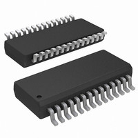
IC CTRLR DDR DRAM, SDRAM 28QSOP
Manufacturer
Intersil
Datasheet
1.ISL6539CAZ.pdf
(20 pages)
Specifications of ISL6539CA
Applications
Controller, DDR DRAM, SDRAM
Voltage - Input
3.3 ~ 18 V
Number Of Outputs
2
Voltage - Output
0.9 ~ 5.5 V
Operating Temperature
0°C ~ 70°C
Mounting Type
Surface Mount
Package / Case
28-QSOP
Lead Free Status / RoHS Status
Contains lead / RoHS non-compliant
Available stocks
Company
Part Number
Manufacturer
Quantity
Price
Company:

Part Number:
ISL6539CA
Manufacturer:
INTERSIL
Quantity:
30
Part Number:
ISL6539CAZ
Manufacturer:
INTERSIL
Quantity:
20 000
Part Number:
ISL6539CAZ-T
Manufacturer:
INTERSIL
Quantity:
20 000


Electrical Specifications
NOTES:
Functional Pin Description
GND (Pin 1, 9, 20)
Signal ground for the IC. All three ground pins must be
connected to ground for proper IC operation. Connect to the
ground plane through a path as low in inductance as
possible.
LGATE1, LGATE2 (Pin 2, 27)
Connect these pins to the gates of the corresponding lower
MOSFETs. These pins provide the PWM-controlled gate
drive for the lower MOSFETs.
PGND1, PGND2 (Pin 3, 26)
These pins provide the return connection for lower gate
drivers, and are connected to sources of the lower
MOSFETs of their respective converters. These pins must
PWM CONVERTERS
Load Regulation
VSEN Pin Bias Current
Minimum Duty Cycle
Maximum Duty Cycle
Undervoltage Shut-Down Level
Overvoltage Protection
GATE DRIVERS
Upper Drive Pull-Up Resistance
Upper Drive Pull-Down Resistance
Lower Drive Pull-Up Resistance
Lower Drive Pull-Down Resistance
POWER GOOD AND CONTROL FUNCTIONS
Power Good Lower Threshold
Power Good Higher Threshold
PGOODx Leakage Current
PGOODx Voltage Low
ISEN Sourcing Current
OCSET Sourcing Current Range
EN - Low (Off)
EN - High (On)
DDR - Low (Off)
DDR - High (On)
DDR REF Output Voltage
DDR REF Output Current
3. Limits should be considered typical and are not production tested.
PARAMETER
5
Recommended Operating Conditions, Unless Otherwise Noted. (Continued)
R2UGPUP VCC = 5V
R2UGPDN VCC = 5V
R2LGPUP VCC = 5V
R2LGPDN VCC = 5V
VPGOOD
SYMBOL
VDDREF
IPGLKG
IDDREF
VOVP1
IVSEN
DMAX
VUVL
VPG+
DMIN
VPG
-
(Note 3)
Fraction of the set point; ~2µs noise filter
Fraction of the set point; ~2µs noise filter
Fraction of the set point; ~3µs noise filter.
IPGOOD = -4mA
(Note 3)
DDR = 1, IREF = 0...10mA
DDR = 1 (Note 3)
0.0mA < IVOUT1 <5.0A; 5.0V < VIN <15.0V
Fraction of the set point; ~3µs noise filter
VPULLUP = 5.5V
ISL6539
TEST CONDITIONS
be connected to the ground plane through a path as low in
inductance as possible.
PHASE1, PHASE2 (Pin 4, 25)
The PHASE1 and PHASE2 points are the junction points of
the upper MOSFET sources, output filter inductors, and
lower MOSFET drains. Connect these pins to the respective
converter’s upper MOSFET source.
UGATE1, UGATE2 (Pin 5, 24)
Connect these pins to the gates of the corresponding upper
MOSFETs. These pins provide the PWM-controlled gate
drive for the upper MOSFETs.
BOOT1, BOOT2 (Pin 6, 23)
These pins power the upper MOSFET drivers of the PWM
converter. Connect these pins to the junction of the bootstrap
VOC2
0.99*
MIN
-2.0
110
110
2.0
70
84
2
3
-
-
-
-
-
-
-
-
-
-
-
-
-
VOC2
TYP
115
115
2.3
1.1
0.5
80
87
75
89
10
4
4
4
-
-
-
-
-
-
-
-
VOC2
1.01*
MAX
+2.0
120
260
0.8
0.8
80
92
12
20
8
4
8
3
1
1
-
-
-
-
-
-
April 29, 2010
UNITS
FN9144.6
mA
nA
µA
µA
µA
%
%
%
%
%
%
%
Ω
Ω
Ω
Ω
V
V
V
V
V
V
Related parts for ISL6539CA
Image
Part Number
Description
Manufacturer
Datasheet
Request
R

Part Number:
Description:
Intersil Corporation [CMOS Serial Controller Interface]
Manufacturer:
Intersil Corporation
Datasheet:
Part Number:
Description:
Manufacturer:
Intersil Corporation
Datasheet:
Part Number:
Description:
357-036-542-201 CARDEDGE 36POS DL .156 BLK LOPRO
Manufacturer:
Intersil Corporation
Datasheet:
Part Number:
Description:
1024-Word x 4-Bit LSI Static RAM
Manufacturer:
Intersil Corporation
Datasheet:
Part Number:
Description:
General Purpose NPN Transistor Arrays FN341.4
Manufacturer:
Intersil Corporation
Datasheet:
Part Number:
Description:
CMOS 16-Bit Microprocessor
Manufacturer:
Intersil Corporation
Datasheet:
Part Number:
Description:
Manufacturer:
Intersil Corporation
Datasheet:
Part Number:
Description:
Manufacturer:
Intersil Corporation
Datasheet:
Part Number:
Description:
Manufacturer:
Intersil Corporation
Datasheet:
Part Number:
Description:
Manufacturer:
Intersil Corporation
Datasheet:
Part Number:
Description:
CMOS 6-Bit Latch and Decoder Memory Interfaces
Manufacturer:
Intersil Corporation
Datasheet:
Part Number:
Description:
CA3046General Purpose NPN Transistor Arrays
Manufacturer:
Intersil Corporation
Datasheet:
Part Number:
Description:
Manufacturer:
Intersil Corporation
Datasheet:
Part Number:
Description:
TR909 DLC/FLC SLIC with Low Power Standby
Manufacturer:
Intersil Corporation
Datasheet:
Part Number:
Description:
Manufacturer:
Intersil Corporation
Datasheet: