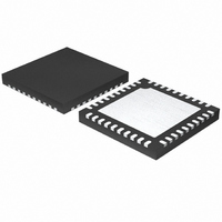
ISL6566CR-T Intersil, ISL6566CR-T Datasheet - Page 21

ISL6566CR-T
Manufacturer Part Number
ISL6566CR-T
Description
IC CTRLR PWM BUCK 3PHASE 40-QFN
Manufacturer
Intersil
Datasheet
1.ISL6566CRZ-TR5184.pdf
(29 pages)
Specifications of ISL6566CR-T
Applications
Controller, Intel VRM9, VRM10, and AMD Hammer Applications
Voltage - Input
3 ~ 12 V
Number Of Outputs
1
Voltage - Output
0.84 ~ 1.6 V
Operating Temperature
0°C ~ 70°C
Mounting Type
Surface Mount
Package / Case
40-VFQFN, 40-VFQFPN
Lead Free Status / RoHS Status
Contains lead / RoHS non-compliant
Available stocks
Company
Part Number
Manufacturer
Quantity
Price
Company:
Part Number:
ISL6566CR-T
Manufacturer:
INTERSIL
Quantity:
7 897
UPPER MOSFET POWER CALCULATION
In addition to r
MOSFET losses are due to currents conducted across the
input voltage (V
higher portion of the upper-MOSFET losses are dependent
on switching frequency, the power calculation is more
complex. Upper MOSFET losses can be divided into
separate components involving the upper-MOSFET
switching times, the lower-MOSFET body-diode reverse-
recovery charge, Q
conduction loss.
When the upper MOSFET turns off, the lower MOSFET does
not conduct any portion of the inductor current until the
voltage at the phase node falls below ground. Once the
lower MOSFET begins conducting, the current in the upper
MOSFET falls to zero as the current in the lower MOSFET
ramps up to assume the full inductor current. In Equation 17,
the required time for this commutation is t
approximated associated power loss is P
At turn on, the upper MOSFET begins to conduct and this
transition occurs over a time t
approximate power loss is P
A third component involves the lower MOSFET reverse-
recovery charge, Q
commutated to the upper MOSFET before the lower-
MOSFET body diode can recover all of Q
through the upper MOSFET across VIN. The power
dissipated as a result is P
Finally, the resistive part of the upper MOSFET is given in
Equation 20 as P
The total power dissipated by the upper MOSFET at full load
can now be approximated as the summation of the results
from Equations 17, 18, 19 and 20. Since the power
equations depend on MOSFET parameters, choosing the
correct MOSFETs can be an iterative process involving
repetitive solutions to the loss equations for different
MOSFETs and different switching frequencies.
Package Power Dissipation
When choosing MOSFETs it is important to consider the
amount of power being dissipated in the integrated drivers
located in the controller. Since there are a total of three
drivers in the controller package, the total power dissipated
P
P
P
P
P
UP 1 ,
UP 2 ,
UP 2 ,
UP 3 ,
UP 4 ,
≈
≈
≈
≈
=
V
r
V
V
DS ON
V
IN
IN
IN
IN
(
I
----- -
Q
I
I
----- -
----- -
N
N
N
M
M
M
rr
DS(ON)
)
+
–
–
IN
f
S
I
-------- -
I
I
-------- -
-------- -
UP,4
PP
PP
PP
I
----- -
) during switching. Since a substantially
2
2
2
N
M
rr
rr
t
t
t
, and the upper MOSFET r
. Since the inductor current has fully
2
.
d
losses, a large portion of the upper-
----
----
----
2
2
2
2
2
1
+
I
--------- -
f
f
f
UP,3
PP
12
S
S
S
2
UP,2
21
2
.
. In Equation 18, the
.
UP,1
1
rr
, it is conducted
and the
.
DS(ON)
(EQ. 17)
(EQ. 18)
(EQ. 19)
(EQ. 20)
ISL6566
by all three drivers must be less than the maximum
allowable power dissipation for the QFN package.
Calculating the power dissipation in the drivers for a desired
application is critical to ensure safe operation. Exceeding the
maximum allowable power dissipation level will push the IC
beyond the maximum recommended operating junction
temperature of 125°C. The maximum allowable IC power
dissipation for the 6x6 QFN package is approximately 4W at
room temperature. See Layout Considerations paragraph for
thermal transfer improvement suggestions.
When designing the ISL6566 into an application, it is
recommended that the following calculation is used to
ensure safe operation at the desired frequency for the
selected MOSFETs. The total gate drive power losses,
P
integrated driver’s internal circuitry and their corresponding
average driver current can be estimated with Equations 21
and 22, respectively.
In Equations 21 and 22, P
power loss and P
loss; the gate charge (Q
particular gate to source drive voltage PVCC in the
corresponding MOSFET data sheet; I
quiescent current with no load at both drive outputs; N
and N
phase, respectively; N
phases. The I
controller without capacitive load and is typically 75mW at
300kHz.
P
PVCC
P
I
P
DR
Qg_TOT
Qg_Q1
Qg_Q2
Qg_TOT
FIGURE 15. TYPICAL UPPER-GATE DRIVE TURN-ON PATH
=
Q2
PHASE
3
-- - Q
2
=
=
, due to the gate charge of MOSFETs and the
•
are the number of upper and lower MOSFETs per
=
BOOT
3
-- - Q
2
Q
R
R
P
•
G2
G1
LO1
HI1
Qg_Q1
Q*
•
•
G1
VCC product is the quiescent power of the
PVCC
N
Qg_Q2
Q1
•
+
PVCC
+
UGATE
P
PHASE
Qg_Q2
Q
•
G1
G2
is the total lower gate drive power
F
Qg_Q1
SW
•
and Q
•
F
N
SW
+
•
is the number of active
Q2
N
R
I
Q
G1
Q2
•
is the total upper gate drive
G2
G
•
N
•
VCC
•
Q1
N
) is defined at the
R
N
C
PHASE
Q
GI1
GD
PHASE
•
C
is the driver total
N
GS
PHASE
•
S
F
SW
D
March 9, 2006
+
Q1
I
C
(EQ. 22)
(EQ. 21)
Q
FN9178.4
DS
Q1


