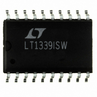
LT1339ISW#PBF Linear Technology, LT1339ISW#PBF Datasheet - Page 14

LT1339ISW#PBF
Manufacturer Part Number
LT1339ISW#PBF
Description
IC DC/DC CONTROLLER HIPWR 20SOIC
Manufacturer
Linear Technology
Type
Step-Up (Boost)r
Datasheet
1.LT1339CNPBF.pdf
(20 pages)
Specifications of LT1339ISW#PBF
Internal Switch(s)
No
Synchronous Rectifier
Yes
Number Of Outputs
1
Current - Output
65mA
Frequency - Switching
150kHz
Voltage - Input
Up to 60V
Operating Temperature
-40°C ~ 85°C
Mounting Type
Surface Mount
Package / Case
20-SOIC (7.5mm Width)
Primary Input Voltage
60V
No. Of Outputs
1
Output Voltage
54V
Output Current
65mA
No. Of Pins
20
Operating Temperature Range
-40°C To +85°C
Msl
MSL 1 - Unlimited
Rohs Compliant
Yes
Lead Free Status / RoHS Status
Lead free / RoHS Compliant
Voltage - Output
-
Power - Output
-
Available stocks
Company
Part Number
Manufacturer
Quantity
Price
APPLICATIONS
LT1339
further increasing the effective compensation slope up to
20% for a given setting.
Design Example:
The minimum inductor usable with no additional slope
compensation is:
Since L = 5 H is less than L
sation is necessary. The total slope compensation
required is:
Subtracting the internally generated slope compensation
and solving for the required effective resistance at SL/ADJ
yields:
Setting the resistor divider reference voltage at 2V assures
that the additional compensation waveform will be
enabled at 75% duty cycle. As shown in Figure 7a, using
R
voltage and has a R
requirements. Figure 7b shows the slope compensation
effective waveforms both with and without the SL/ADJ
external resistors.
Power MOSFET and Catch Diode Selection
External N-channel MOSFET switches are used with the
LT1339. The positive gate-source drive voltage of the
LT1339 for both switches is roughly equivalent to the
12V
can be used.
14
SL1
V
V
R
f
L = 5 H
L
R
S
O
IN
IN
OUT
SENSE
MIN
EQ
X
= 100kHz
= 45k and R
= 20V
supply voltage, so standard threshold MOSFETs
= 15V (DC = 0.75)
20
5
= 0.01
2 10
20
V
H
0 084 100000
V
1 5 1
6
0 01
SL2
U
R
EQ
SENSE
2500
= 30k sets the desired reference
of 18k, which meets both design
INFORMATION
1 5 1
U
MIN
2 10
f
O
, additional slope compen-
0 084
6
W
11 9
f
O
Amp/s
H
21 5
U
k
Selection criteria for the power MOSFETs include the “ON”
resistance (R
maximum drain-source voltage (V
output current.
The power FETs selected must have a maximum operating
V
must exceed the 12V
Once voltage requirements have been determined, R
can be selected based on allowable power dissipation and
required output current.
In an LT1339 buck converter, the average inductor current
is equal to the DC load current. The average currents
through the main and synchronous switches are:
The R
calculated using the relation:
DSS
I
I
P
MAIN
SYNC
LOSS
exceeding the maximum V
DS(ON)
Figure 7a. External Slope Compensation Resistors
2.5V
0.8V
2V
= (I
= (I
= (I
Figure 7b. Slope Compensation Waveforms
LOAD
LOAD
required for a given conduction loss can be
SWITCH
DS(ON)
)(DC)
)(1 – DC)
R
45k
R
30k
SL1
SL2
), reverse transfer capacitance (C
)
DC = 0.75
2
IN
(R
2
4
5V
SL/ADJ
supply voltage.
DS(ON)
REF
LT1339
)
IN
1339 • F07a
. V
GS
DSS
voltage maximum
) and maximum
(0.084 + 0.139)(f
1339 • F07b
R
sn1339 1339fas
SENSE
(0.084)(f
R
SENSE
DS(ON)
RSS
O
O
)
)
),


