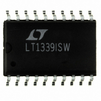
LT1339ISW#PBF Linear Technology, LT1339ISW#PBF Datasheet - Page 16

LT1339ISW#PBF
Manufacturer Part Number
LT1339ISW#PBF
Description
IC DC/DC CONTROLLER HIPWR 20SOIC
Manufacturer
Linear Technology
Type
Step-Up (Boost)r
Datasheet
1.LT1339CNPBF.pdf
(20 pages)
Specifications of LT1339ISW#PBF
Internal Switch(s)
No
Synchronous Rectifier
Yes
Number Of Outputs
1
Current - Output
65mA
Frequency - Switching
150kHz
Voltage - Input
Up to 60V
Operating Temperature
-40°C ~ 85°C
Mounting Type
Surface Mount
Package / Case
20-SOIC (7.5mm Width)
Primary Input Voltage
60V
No. Of Outputs
1
Output Voltage
54V
Output Current
65mA
No. Of Pins
20
Operating Temperature Range
-40°C To +85°C
Msl
MSL 1 - Unlimited
Rohs Compliant
Yes
Lead Free Status / RoHS Status
Lead free / RoHS Compliant
Voltage - Output
-
Power - Output
-
Available stocks
Company
Part Number
Manufacturer
Quantity
Price
LT1339
APPLICATIONS
is also small. However, since the FET gate must switch up
past the 48V input voltage, transition loss can become a
significant factor. In such a case, it is often prudent to take
the increased I
C
Gate Drive Buffers
The LT1339 is designed to drive relatively large capacitive
loads. However, in certain applications, efficiency im-
provements can be realized by adding an external buffer
stage to drive the gates of the FET switches. When the
switch gates load the driver outputs such that rise/fall
times exceed about 100ns, buffers can sometimes result
in efficiency gains. Buffers also reduce the effect of back
injection into the bottom side driver output due to coupling
of switch node transitions through the switch FET C
Paying the Physicists
In high power synchronous buck configurations, certain
physical characteristics of the external MOSFET switches
can impact conversion efficiency. As the input voltage
approaches about 30V, the bottom MOSFETs will begin to
exhibit “phantom turn-on.” This phenomenon is caused
by coupling of the instantaneous voltage step on the
bottom side switch drain through C
gate, yielding internal localized gate-source voltages above
the turn-on threshold of the FET. This generates a shoot-
through blip that ultimately eats away at efficiency num-
bers. In Figure 8 a negative prebias circuit is added to the
bottom side gate. The addition of this 3V of negative
offset to the bottom gate drive provides additional off-
state voltage range to prevent phantom turn-on.
16
RSS
Figure 8. Bottom Side Driver Negative Prebias Circuit
and thus, the associated transition losses.
LT1339
2
R loss of a smaller FET in order to reduce
12V
PGND
BG
TS
U
IN
INFORMATION
U
ZTX649
ZTX749
3.3V
1 F
W
MILLER
10k
D1N914
to the device
U
1339 F08
MILLER
.
This type of prebias circuit is used in the 48V to 5V, 50A
converter pictured in the Typical Applications section.
As currents increase beyond the 10A to 15A range, the
bottom side FET body diode experiences hard turn-on
during switch dead time due to local current loop induc-
tance preventing the timely transfer of charge to the
Schottky catch diode. The charge current required to
commutate this body diode creates a high dV/dt Schottky
avalanche when the diode charge is finally exhausted (due
to an effective inductor current discontinuity at the
moment the body diode no longer requires charge). This
generates an increased turn-on power burst in the topside
switch, causing additional conversion efficiency loss. This
effect of this parasitic inductance can be reduced by using
FETKEY
diodes internal to their packages. FETKEY MOSFETs are
not available for high voltages, so as input voltage contin-
ues to increase, they can no longer be used. Because this
necessitates the use of discrete FETs and Schottkys,
interdigitation of a number of smaller devices is required
to minimize parasitic inductances. This technique is also
used in the 48V to 5V, 50A converter shown in the Typical
Applications section.
Optimizing Transient Response—Compensation
Component Values
The dominant compensation point for an LT1339 con-
verter is the V
pin is connected to a series RC network, R
infinite permutations of input/output filtering, capacitor
ESR, input voltage, load current, etc. make for an empirical
method of optimizing loop response for a specific set of
conditions.
Loop response can be observed by injecting a step change
in load current. This can be achieved by using a switchable
load. With the load switching, the transient response of the
output voltage can be observed with an oscilloscope.
Iterating through RC combinations will yield optimized
response. Refer to LTC Application Note 19 in 1990 Linear
Applications Handbook, Volume 1 for more information.
FETKEY is a trademark of International Rectifier Corporation.
TM
MOSFETs, which have parallel catch Schottky
C
pin (Pin 7), or error amplifier output. This
VC
and C
sn1339 1339fas
VC
. The


