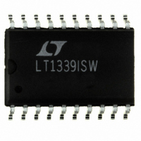
LT1339ISW#PBF Linear Technology, LT1339ISW#PBF Datasheet - Page 15

LT1339ISW#PBF
Manufacturer Part Number
LT1339ISW#PBF
Description
IC DC/DC CONTROLLER HIPWR 20SOIC
Manufacturer
Linear Technology
Type
Step-Up (Boost)r
Datasheet
1.LT1339CNPBF.pdf
(20 pages)
Specifications of LT1339ISW#PBF
Internal Switch(s)
No
Synchronous Rectifier
Yes
Number Of Outputs
1
Current - Output
65mA
Frequency - Switching
150kHz
Voltage - Input
Up to 60V
Operating Temperature
-40°C ~ 85°C
Mounting Type
Surface Mount
Package / Case
20-SOIC (7.5mm Width)
Primary Input Voltage
60V
No. Of Outputs
1
Output Voltage
54V
Output Current
65mA
No. Of Pins
20
Operating Temperature Range
-40°C To +85°C
Msl
MSL 1 - Unlimited
Rohs Compliant
Yes
Lead Free Status / RoHS Status
Lead free / RoHS Compliant
Voltage - Output
-
Power - Output
-
Available stocks
Company
Part Number
Manufacturer
Quantity
Price
APPLICATIONS
In high voltage applications (V
is required to slew very large voltages. As V
transition losses increase through a square relation, until
it becomes the dominant power loss term in the main
switch. This transition loss takes the form:
where k is a constant inversely related to the gate drive
current, approximated by k = 2 in LT1339 applications.
The maximum power loss terms for the switches are thus:
The (1 + ) term in the above relations is the temperature
dependency of R
normalized R
data sheet.
In some applications, parasitic FET capacitances couple
the negative going switch node transient onto the bottom
gate drive pin of the LT1339, causing a negative voltage in
excess of the Absolute Maximum Rating to be imposed on
that pin. Connection of a catch Schottky (rated to about 1A
is typically sufficient) from this pin to ground will eliminate
this effect.
C
The large currents typical of LT1339 applications require
special consideration for the converter input and output
supply decoupling capacitors. Under normal steady state
operation, the source current of the main switch MOSFET
is a square wave of duty cycle V
current is provided by the input bypass capacitor. To
prevent large input voltage transients and avoid bypass
capacitor heating, a low ESR input capacitor sized for the
maximum RMS current must be used. This maximum
capacitor RMS current follows the relation:
which peaks at a 50% duty cycle, when I
Capacitor ripple current ratings are often based on only
IN
P
P
P
I
RMS
and C
TR
MAIN
SYNC
(k)(V
= (DC)(I
= (1 – DC)(I
OUT
2(V
I
MAX
DS(ON)
Supply Decoupling Capacitor Selection
IN
IN
)
2
)
DS(ON)
MAX
(I
2
V
(I
U
MAX
OUT
vs Temperature curve in a MOSFET
MAX
)
MAX
2
)(C
(1 + )(R
, typically given in the form of a
)(C
V
INFORMATION
V
)
U
IN
2
IN
RSS
(1 + )(R
RSS
–
IN
)(f
)(f
V
> 20V), the topside switch
O
OUT
DS(ON)
O
)
)
OUT
W
DS(ON)
/ 1 2
/V
) +
IN
. Most of this
RMS
)
IN
increases,
U
= I
MAX
/2.
2000 hours (three months) lifetime; it is advisable to
derate either the ESR or temperature rating of the capaci-
tor for increased MTBF of the regulator.
The output capacitor in a buck converter generally has
much less ripple current than the input capacitor. Peak-to-
peak ripple current is equal to that in the inductor ( I
typically a fraction of the load current. C
reduce output voltage ripple to a desirable value given an
expected output ripple current. Output ripple ( V
approximated by:
where f
Efficiency Considerations and Heat Dissipation
High output power applications have inherent concerns
regarding power dissipation in converter components.
Although high efficiencies are achieved using the LT1339,
the power dissipated in the converter climbs to relatively
high values when the load draws large amounts of power.
Even at 90% efficiency, an application that provides 500W
to the load has conversion loss of 55W.
I
inductor series resistance create substantial losses under
high currents. Generally, the dominant I
in the FET switches. Loss in each switch is proportional to
the conduction time of that switch. For example, in a 48V
to 5V converter the synchronous FET conducts load cur-
rent for almost 90% of the cycle time and thus, requires
greater consideration for dissipating I
Gate charge/discharge current creates additional current
drain on the 12V supply. If powered from a high voltage
input through a linear regulator, the losses in that regula-
tor device can become significant. A supply solution
bootstrapped from the output would draw current from a
lower voltage source and reduce this loss component.
Transition losses are significant in the topside switch FET
when high V
estimated as:
Since the conduction time in the main switch of a 48V to
5V converter is small, the I
2
R dissipation through the switches, sense resistor and
P
TLOSS
V
OUT
O
= operating frequency.
IN
2(V
I
L
voltages are used. Transition losses can be
{ESR + [(4)(f
IN
)
2
(I
MAX
)(C
2
R loss in the main switch FET
O
RSS
)
•
)(f
C
OUT
O
)
]
2
–1
R power.
OUT
2
}
R loss is evident
is selected to
LT1339
sn1339 1339fas
15
OUT
) is
L
),


