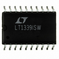
LT1339ISW#PBF Linear Technology, LT1339ISW#PBF Datasheet - Page 7

LT1339ISW#PBF
Manufacturer Part Number
LT1339ISW#PBF
Description
IC DC/DC CONTROLLER HIPWR 20SOIC
Manufacturer
Linear Technology
Type
Step-Up (Boost)r
Datasheet
1.LT1339CNPBF.pdf
(20 pages)
Specifications of LT1339ISW#PBF
Internal Switch(s)
No
Synchronous Rectifier
Yes
Number Of Outputs
1
Current - Output
65mA
Frequency - Switching
150kHz
Voltage - Input
Up to 60V
Operating Temperature
-40°C ~ 85°C
Mounting Type
Surface Mount
Package / Case
20-SOIC (7.5mm Width)
Primary Input Voltage
60V
No. Of Outputs
1
Output Voltage
54V
Output Current
65mA
No. Of Pins
20
Operating Temperature Range
-40°C To +85°C
Msl
MSL 1 - Unlimited
Rohs Compliant
Yes
Lead Free Status / RoHS Status
Lead free / RoHS Compliant
Voltage - Output
-
Power - Output
-
Available stocks
Company
Part Number
Manufacturer
Quantity
Price
PIN
SYNC (Pin 1): Oscillator Synchronization Pin with TTL-
Level Compatible Input. Input drives internal rising edge
triggered one-shot; sync signal on/off times should be
internal pull-up. Connect to SGND if not used.
5V
of external loads up to 10mA DC. (Reference is not
available in shutdown.) Typically bypassed with 1 F
capacitor to SGND.
CT (Pin 3): Oscillator Timing Pin. Connect a capacitor
(C
supply. Typical values are CT = 1000pF and 10k
SL/ADJ (Pin 4): Slope Compensation Adjustment.
Allows increased slope compensation for certain high
duty cycle applications. Resistive loading of the pin
increases effective slope compensation. A resistor
divider from the 5V
tional slope compensation to specific regions in each
switch cycle. Pin can be floated or connected to 5V
no additional slope compensation is required. (See
Applications Information section for slope compensa-
tion details.)
I
quency response characteristic is set using the 50k
output impedance and external capacitor to ground.
Averaging roll-off typically set at 1 to 2 orders of magni-
tude under switching frequency. (Typical capacitor value
~1000pF for f
disable the average current limit function.
SS (Pin 6): Soft Start. Generates ramping threshold for
regulator current limit during start-up and after UVLO
event by sourcing about 8 A into an external capacitor.
V
dominant compensation in power supply regulation feed-
back loop to provide optimum transient response. (See
Applications Information section for compensation de-
tails.)
SGND (Pin 8): Small-Signal Ground. Connect to negative
terminal of C
V
voltage feedback input node for regulator loop. Pin
sources about 0.5 A DC bias current to protect from an
open feedback path condition.
AVG
1 s (10% to 90% DC at 100kHz). Does not contain
C
FB
30k.
CT
REF
U
(Pin 7): Error Amplifier Output. RC load creates
) to ground and a pull-up resistor (R
(Pin 9): Error Amplifier Inverting Input. Used as
(Pin 5): Average Current Limit Integration. Fre-
FUNCTIONS
(Pin 2): 5V Output Reference. Allows connection
U
OUT
O
= 100kHz.) Shorting this pin to SGND will
.
REF
U
pin can tailor the onset of addi-
CT
) to the 5V
REF
R
REF
CT
if
V
Decoupling. Connect a capacitor to signal ground. (Typi-
cal capacitor value ~0.1 F.)
SENSE
Input. Connect to most positive (DC) terminal of current
sense resistor.
SENSE
Input. Connect to most negative (DC) terminal of current
sense resistor.
RUN/SHDN (Pin 13): Precision Referenced Shutdown.
Can be used as logic level input for shutdown control or
as an analog monitor for input supply undervoltage
protection, etc. IC is enabled when RUN/SHDN pin rising
edge exceeds 1.25V. About 25mV of hysteresis helps
assure stable mode switching. All internal functions are
disabled in shutdown mode. If this function is not
desired, connect RUN/SHDN to 12V
a 100k resistor). See Applications Information section.
PHASE (Pin 14): Output Driver Phase Control. If Pin 14
is not connected (floating), the topside driver operates
the main switch, with the bottom side driver operating
the synchronous switch. Shorting Pin 14 to ground
reverses the roles of the output drivers. PHASE is typi-
cally shorted to ground for inverting and boost configu-
rations. Positive buck configuration requires the PHASE
pin to float. See Applications Information section.
PGND (Pin 15): Power Ground. References the bottom
side output switch and internal driver control circuits.
Connect with low impedance trace to V
capacitor negative (ground) terminal.
BG (Pin 16): Bottom Side Output Driver. Connects to gate
of bottom side external power FET.
12V
least 1 F to PGND.
TS (Pin 18): Boost Output Driver Reference. Typically
connects to source of topside external power FET and
inductive switch node.
TG (Pin 19): Topside (Boost) Output Driver. Connects to
gate of topside external power FET.
V
via 1 F capacitor tied to switch node (Pin 18) and
Schottky diode connected to the 12V
REF
BOOST
IN
(Pin 10): Bandgap Generated Voltage Reference
(Pin 17): 12V Power Supply Input. Bypass with at
+
–
(Pin 20): Topside Power Supply. Bootstrapped
(Pin 12): Current Sense Amplifier Noninverting
(Pin 11): Current Sense Amplifier Inverting
IN
IN
(typically through
supply.
IN
LT1339
decoupling
sn1339 1339fas
7


