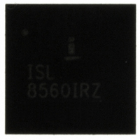
ISL8560IRZ Intersil, ISL8560IRZ Datasheet - Page 4

ISL8560IRZ
Manufacturer Part Number
ISL8560IRZ
Description
IC REG 2A DC/DC STEP-DN 20-QFN
Manufacturer
Intersil
Type
Step-Down (Buck)r
Datasheet
1.ISL8560IRZ.pdf
(17 pages)
Specifications of ISL8560IRZ
Internal Switch(s)
Yes
Synchronous Rectifier
Yes
Number Of Outputs
1
Voltage - Output
1.21 ~ 55 V
Current - Output
2A
Frequency - Switching
100kHz ~ 600kHz
Voltage - Input
9 ~ 60 V
Operating Temperature
-40°C ~ 85°C
Mounting Type
Surface Mount
Package / Case
20-VQFN Exposed Pad, 20-HVQFN, 20-SQFN, 20-DHVQFN
Power - Output
3W
Rohs Compliant
Yes
Lead Free Status / RoHS Status
Lead free / RoHS Compliant
Available stocks
Company
Part Number
Manufacturer
Quantity
Price
Company:
Part Number:
ISL8560IRZ
Manufacturer:
Intersil
Quantity:
48
Company:
Part Number:
ISL8560IRZ
Manufacturer:
Intersil
Quantity:
135
Pin Descriptions
LX (Pins 1, 2, 15, 16)
There are four output pins that must be connected together
externally in normal operation.
BOOT (Pin 3)
A capacitor is connected from this pin to the output pin. An
internal 10V supply and an internal Schottky diode provide
the high side voltage to drive the gate of the output DMOS
device.
EN (Pin 4)
The EN input will disable the part and shut-down all function
when it is held high or left OPEN. The EN current will be
10µA typical. An internal pull-up resistor will hold the pin
high. When EN = Low, the part is enabled. Connect to GND
for auto start-up.
VCC5 (Pin 5)
VCC5 is the +5.0V output pin which provides an output of an
internal supply for supply filtering purposes. A 1µF capacitor
should be connected from this pin to GND. Internal VDD
supply is set at 5.0V (not planned that the user would use
this supply).
SYNC (Pin 6)
This pin provides a digital input pin to synchronize the
internal oscillator to an external signal. When the sync
function is not used, this pin can be left open or tied to GND.
If the sync function is used, the RTCT timing must be set to a
frequency lower than the sync input frequency. The
termination of the ramp is synchronized with the rising edge
of the sync input signal. There are no duty cycle restrictions
on the input sync signal. Input thresholds are TTL
compatible.
RTCT (Pin 7)
A resistor to VIN and a capacitor to GND determine the
frequency of the saw-tooth oscillator. Resistor range is
R = 20k to 100k. Capacitor range is C = 470pF to 1.2nF. The
oscillator amplitude will vary from approximately 0.9V to 10V
as V
frequency and provide feed forward. The oscillator will have
a fixed off time, which will establish the maximum on time for
the regulator. This off time will be <200ns. The maximum
duty cycle for a 500kHz system will therefore be
approximately 90% as the frequency of the maximum duty
cycle will increase (95% for 250kHz system). The minimum
duty cycle is zero.
IN
changes from 8.5V to 60V to maintain constant
4
ISL8560
SGND (Pin 8)
The SGND terminal of the ISL8560 provides the return path
for the control and monitor portions of the IC.
FB (Pin 9)
This is the feedback pin. The feedback ratio is set by an
external resistor divider connected to the load.
COMP (Pin 10)
This pin is connected to the output of the Error Amplifier and
is used to compensate the loop. The Error Amplifier is a GM
amplifier.
REF (Pin 11)
1.20V reference output. Bypass to GND with 0.01µF
capacitor.
PGOOD (Pin 12)
This pin is an open drain output that is turned on when the
feedback voltage is more than ±10% from the reference
voltage, indicating that the output is not within 10% of set
point.
PGND (Pin 13)
This pin is used as the ground connection of the power train.
SS (Pin 14)
A capacitor is connected from this pin to GND to determine
the soft-start timing. The soft-start pin internal charging
current is 10µA.
VIN (Pins 17, 18, 19, 20)
The input supply for the PWM regulator power stage.
Connected to DRAIN of the high side MOSFET.
September 19, 2008
FN9244.7


