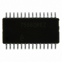
EL7566DREZ Intersil, EL7566DREZ Datasheet - Page 13

EL7566DREZ
Manufacturer Part Number
EL7566DREZ
Description
IC REG 6A DC-DC STEP DN 28HTSSOP
Manufacturer
Intersil
Type
Step-Down (Buck)r
Datasheet
1.EL7566DREZ.pdf
(14 pages)
Specifications of EL7566DREZ
Internal Switch(s)
Yes
Synchronous Rectifier
Yes
Number Of Outputs
1
Voltage - Output
0.8 ~ 6 V
Current - Output
6A
Frequency - Switching
370kHz
Voltage - Input
3 ~ 6 V
Operating Temperature
0°C ~ 85°C
Mounting Type
Surface Mount
Package / Case
28-TSSOP Exposed Pad, 28-eTSSOP, 28-HTSSOP
Lead Free Status / RoHS Status
Lead free / RoHS Compliant
Power - Output
-
Available stocks
Company
Part Number
Manufacturer
Quantity
Price
Company:
Part Number:
EL7566DREZ
Manufacturer:
INTERSIL
Quantity:
114
Part Number:
EL7566DREZ
Manufacturer:
EL
Quantity:
20 000
Company:
Part Number:
EL7566DREZ-T7
Manufacturer:
Intersil
Quantity:
4 050
For convenience, Table 3 lists the compensation values for
frequently used output voltages.
Thermal Management
The EL7566 is packaged in a thermally-efficient HTSSOP-28
package, which utilizes the exposed thermal pad at the
bottom to spread heat through PCB metal.
Therefore:
The thermal resistance for this package is as low as 26°C/W
for 2 layer PCB of 0.39" thickness (See Figure 9). The actual
junction temperature can be measured at V
The thermal performance of the IC is heavily dependent on
the layout of the PCB. The user should exercise care during
the design phase to ensure the IC will operate within the
recommended environmental conditions.
1. The thermal pad must be soldered to the PCB.
2. Maximize the PCB area.
3. If a multiple layer PCB is used, thermal vias (13 to 25 mil)
must be placed underneath the thermal pad to connect to
ground plane(s). Do not place thermal reliefs on the vias.
Figure 25 shows a typical connection.
FIGURE 25. PCB LAYOUT - 28-PIN HTSSOP PACKAGE
COMPONENT SIDE
V
CONNECTION
O
3.3
2.5
1.8
1.5
1.2
0.8
1
(V)
TABLE 3. COMPENSATION VALUES
R
C
13.7
10.5
7.68
6.49
5.23
4.42
3.57
13
(kΩ)
GROUND PLANE
CONNECTION
TJ
pin.
C
8200
8200
8200
8200
8200
8200
8200
C
(pF)
EL7566
Layout Considerations
The layout is very important for the converter to function
properly. Follow these tips for best performance:
The demo board is a good example of layout based on this
outline. Please refer to the EL7566 Application Brief.
1. Separate the Power Ground ( ) and Signal Ground (
2. Place the input capacitor(s) as close to V
3. Make as small as possible the loop from LX pins to L to
4. Place R
5. Maximize the copper area around the PGND pins; do not
6. Thermal pad should be soldered to PCB. Place several
connect them only at one point right at the SGND pin
pins as possible
C
place thermal relief around them
via holes under the chip to the ground plane to help heat
dissipation
O
to PGND pins
1
and R
2
pins as close to the FB pin as possible
IN
and PGND
May 8, 2006
FN7102.7
);


