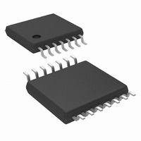
LM5010AQ0MH/NOPB National Semiconductor, LM5010AQ0MH/NOPB Datasheet

LM5010AQ0MH/NOPB
Specifications of LM5010AQ0MH/NOPB
LM5010AQ0MH
Related parts for LM5010AQ0MH/NOPB
LM5010AQ0MH/NOPB Summary of contents
Page 1
... The valley current limit detection is set at 1.25A. Ad- ditional features include: VCC under-voltage lock-out, thermal shutdown, gate drive under-voltage lock-out, and maximum duty cycle limiter. Basic Step Down Regulator © 2008 National Semiconductor Corporation Features ■ Wide 6V to 75V Input Voltage Range ■ ...
Page 2
Connection Diagrams Ordering Information Order Number Package Type LM5010ASD LLP-10 (4x4) LM5010ASDX LLP-10 (4x4) LM5010AMH TSSOP-14EP LM5010AMHE TSSOP-14EP LM5010AMHX TSSOP-14EP LM5010AQ1MH TSSOP-14EP LM5010AQ1MHX TSSOP-14EP LM5010AQ0MH TSSOP-14EP LM5010AQ0MHX TSSOP-14EP *Automotive Grade (Q) product incorporates enhanced manufacturing and support processes for the ...
Page 3
Pin Descriptions Pin Number Name LLP-10 TSSOP- BST 3 4 ISEN 4 5 SGND 5 6 RTN RON/ VCC 10 13 VIN 1,7,8, ...
Page 4
... Absolute Maximum Ratings If Military/Aerospace specified devices are required, please contact the National Semiconductor Sales Office/ Distributors for availability and specifications. VIN to RTN BST to RTN SW to RTN (Steady State) BST to VCC BST to SW VCC to RTN SGND to RTN SS to RTN Electrical Charateristics over the full Operating Junction Temperature (T statistical correlation ...
Page 5
... Device thermal limitations limit external loading. CC Note 4: For detailed information on soldering plastic TSSOP and LLP packages refer to the Packaging Data Book available from National Semiconductor Corporation. Note 5: Typical specifications represent the most likely parametric norm at 25°C operation. ...
Page 6
Typical Performance Characteristics Externally Applied V CC Voltage at RON/SD Pin www.national.com IN 20153804 CC 20153806 20153808 20153805 On-Time vs V and 20153807 I vs ...
Page 7
Block Diagram 7 20153844 www.national.com ...
Page 8
Functional Description The LM5010A Step Down Switching Regulator features all the functions needed to implement a low cost, efficient buck DC-DC converter capable of supplying in excess the load. This high voltage regulator integrates an 80V N-Channel ...
Page 9
ESR is insufficient additional series resistance may be required (R3 in the Block Diagram). The LM5010A operates in continuous conduction mode at heavy load currents, and discontinuous conduction mode at light load currents. In continuous conduction mode current al- ...
Page 10
The buck switch remains off until the voltage at FB falls below 2.5V. ON-Time Control The on-time of the internal buck switch is determined by the R resistor and the input voltage ...
Page 11
FIGURE 4. Inductor Current - Current Limit Operation N - Channel Buck Switch and Driver The LM5010A integrates an N-Channel buck switch and as- sociated floating high voltage gate driver. The peak current through the buck switch should not exceed ...
Page 12
To keep the circuit in continuous conduction mode, the max- imum allowed ripple current is twice the minimum load cur- rent, or 400 mAp-p. Using this value of ripple current, the inductor (L1) is calculated using the following: where F ...
Page 13
C3: The capacitor at the VCC pin provides noise filtering and stability, prevents false triggering of the V switch on/off transitions, and limits the peak voltage at V when a high voltage with a short rise time is initially applied ...
Page 14
Item C4 FIGURE 7. Efficiency vs Load Current and V Circuit of Figure 6 FIGURE 8. Frequency vs V Circuit of Figure 6 MINIMUM LOAD CURRENT The ...
Page 15
Cff and reducing R3 to 0.75Ω, the V ripple was reduced by 50%, ranging from 25 mVp-p to OUT 160 mVp-p. FIGURE 11. Low Output Ripple Using Ripple Injection To reduce V ripple further, the circuit ...
Page 16
Physical Dimensions www.national.com inches (millimeters) unless otherwise noted 14-Lead TSSOP Package NS Package Number MXA14A 10-Lead LLP Package NS Package Number SDC10A 16 ...
Page 17
Notes 17 www.national.com ...
Page 18
... For more National Semiconductor product information and proven design tools, visit the following Web sites at: Products Amplifiers www.national.com/amplifiers Audio www.national.com/audio Clock and Timing www.national.com/timing Data Converters www.national.com/adc Interface www.national.com/interface LVDS www.national.com/lvds Power Management www.national.com/power Switching Regulators www.national.com/switchers LDOs www.national.com/ldo LED Lighting www ...


