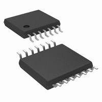
LM5010AQ0MH/NOPB National Semiconductor, LM5010AQ0MH/NOPB Datasheet - Page 4

LM5010AQ0MH/NOPB
Manufacturer Part Number
LM5010AQ0MH/NOPB
Description
IC REG SW 1A SD 14TSSOP AUTO
Manufacturer
National Semiconductor
Type
Step-Down (Buck)r
Datasheet
1.LM5010AMHNOPB.pdf
(18 pages)
Specifications of LM5010AQ0MH/NOPB
Internal Switch(s)
Yes
Synchronous Rectifier
No
Number Of Outputs
1
Voltage - Output
2.5 ~ 70 V
Current - Output
1A
Frequency - Switching
1MHz
Voltage - Input
6 ~ 75 V
Operating Temperature
-40°C ~ 150°C
Mounting Type
Surface Mount
Package / Case
14-TSSOP Exposed Pad, 14-eTSSOP 14-HTSSOP
Package
14TSSOP EP
Minimum Input Voltage
6 V
Maximum Input Voltage
75 V
Switching Frequency
50 to 1000 KHz
Operating Supply Voltage
6 to 75 V
Maximum Output Current
1 A
Output Type
Adjustable
Output Voltage
2.5 to 70 V
Efficiency
91 %
Lead Free Status / RoHS Status
Lead free / RoHS Compliant
Power - Output
-
Other names
*LM5010AQ0MH/NOPB
LM5010AQ0MH
LM5010AQ0MH
www.national.com
V
Switch Characteristics
SOFT-START Pin
Current Limit
On Timer, RON/SD Pin
CC
VIN to RTN
BST to RTN
SW to RTN (Steady State)
BST to VCC
BST to SW
VCC to RTN
SGND to RTN
SS to RTN
Absolute Maximum Ratings
If Military/Aerospace specified devices are required,
please contact the National Semiconductor Sales Office/
Distributors for availability and specifications.
Electrical Charateristics
over the full Operating Junction Temperature (T
statistical correlation. Typical values represent the most likely parametric norm at T
purposes only. Unless otherwise stated the following conditions apply: V
UVLOVcc
UVLO
Symbol
V
R
t
t
Regulator
ON
ON
CC
DS(on)
I
I
LIM
SS
Reg
- 1
- 2
GD
V
V
V
V
V
(0 mA
V
V
threshold
UVLO
UVLO
I
I
Buck Switch R
mA
Gate Drive UVLO
UVLO
Internal current source
Threshold
Resistance from ISEN to SGND
Response time
On-time
On-time
Shutdown threshold
Threshold hysteresis
IN
IN
CC
IN
CC
CC
CC
CC
CC
operating current
shutdown current
- V
regulated output
Bypass Threshold
Bypass Hysteresis
output impedance
current limit (Note 3)
under-voltage lock-out
VCC
VCC
GD
CC
≤
I
hysteresis
CC
hysteresis
filter delay
Parameter
≤
DS(on)
5 mA)
@ I
SW
= 200
Specifications with standard type are for T
-0.3V to +0.3V
(Note 1)
J
I
V
V
V
V
V
V
V
V
100 mV overdrive
Non-switching, FB = 3V
RON/SD = 0V
T
T
V
Current out of I
V
V
Voltage at RON/SD rising
-0.3V to 76V
-0.3V to 90V
-0.3V to 14V
) range. Minimum and Maximum limits are guaranteed through test, design, or
CC
-0.3V to 4V
J
J
IN
IN
IN
IN
IN
IN
CC
CC
BST
IN
IN
≤
≤
= 0 mA, F
Increasing
Decreasing
= 6.0V
= 8.0V
= 48V
= 48V, V
= 10V, R
= 75V, R
Increasing
Decreasing
125°C
150°C
- V
-1.5V
SW
76V
14V
Increasing
CC
ON
ON
S
SEN
< 200 kHz, 6.0V
= 0V
= 200 kΩ
= 200 kΩ
4
Conditions
VIN to SW
All Other Inputs to RTN
ESD Rating (Note 2)
Storage Temperature Range
Lead Temperature (Soldering 4 sec) (Note 4)
VIN Voltage
Junction Temperature
Operating Ratings
Human Body Model
LM5010A/LM5010AQ1
LM5010AQ0
IN
= 48V, R
≤
V
J
ON
IN
= 25°C, and are provided for reference
J
≤
= 200kΩ. See (Note 5).
= 25°C only; limits in boldface type apply
8.5V
0.30
Min
290
6.6
1.7
8.0
2.1
1
(Note 1)
0.21
5.25
0.35
11.5
1.25
2.75
Typ
100
260
180
675
100
400
130
150
390
8.9
3.0
0.7
55
50
15
40
7
3
−40°C to + 125°C
−40°C to + 150°C
-65°C to +150°C
Max
0.80
0.85
1.05
950
200
496
7.4
4.0
1.5
3.4
15
6.0V to 75V
-0.3V to 7V
260°C
Units
Volts
mV
mV
mA
mV
mV
mΩ
mV
76V
2kV
µA
µA
µA
µs
ns
µs
ns
V
Ω
V
Ω
V
A
V


