LM5010AQ0MH/NOPB National Semiconductor, LM5010AQ0MH/NOPB Datasheet - Page 9

LM5010AQ0MH/NOPB
Manufacturer Part Number
LM5010AQ0MH/NOPB
Description
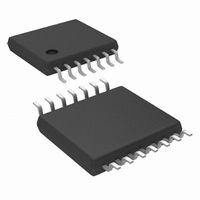
IC REG SW 1A SD 14TSSOP AUTO
Manufacturer
National Semiconductor
Type
Step-Down (Buck)r
Datasheet
1.LM5010AMHNOPB.pdf
(18 pages)
Specifications of LM5010AQ0MH/NOPB
Internal Switch(s)
Yes
Synchronous Rectifier
No
Number Of Outputs
1
Voltage - Output
2.5 ~ 70 V
Current - Output
1A
Frequency - Switching
1MHz
Voltage - Input
6 ~ 75 V
Operating Temperature
-40°C ~ 150°C
Mounting Type
Surface Mount
Package / Case
14-TSSOP Exposed Pad, 14-eTSSOP 14-HTSSOP
Package
14TSSOP EP
Minimum Input Voltage
6 V
Maximum Input Voltage
75 V
Switching Frequency
50 to 1000 KHz
Operating Supply Voltage
6 to 75 V
Maximum Output Current
1 A
Output Type
Adjustable
Output Voltage
2.5 to 70 V
Efficiency
91 %
Lead Free Status / RoHS Status
Lead free / RoHS Compliant
Power - Output
-
Other names
*LM5010AQ0MH/NOPB
LM5010AQ0MH
LM5010AQ0MH
capacitor’s ESR is insufficient additional series resistance
may be required (R3 in the Block Diagram).
The LM5010A operates in continuous conduction mode at
heavy load currents, and discontinuous conduction mode at
light load currents. In continuous conduction mode current al-
ways flows through the inductor, never decaying to zero
during the off-time. In this mode the operating frequency re-
mains relatively constant with load and line variations. The
minimum load current for continuous conduction mode is one-
half the inductor’s ripple current amplitude. The operating
frequency in the continuous conduction mode is calculated as
follows:
The buck switch duty cycle is equal to:
Under light load conditions, the LM5010A operates in discon-
tinuous conduction mode, with zero current flowing through
the inductor for a portion of the off-time. The operating fre-
quency is always lower than that of the continuous conduction
mode, and the switching frequency varies with load current.
Conversion efficiency is maintained at a relatively high level
at light loads since the switching losses diminish as the power
delivered to the load is reduced. The discontinuous mode op-
erating frequency is approximately:
where R
Regulation Comparator
The feedback voltage at the FB pin is compared to the voltage
at the SS pin (2.5V, ±2%). In normal operation an on-time
period is initiated when the voltage at FB falls below 2.5V. The
buck switch conducts for the on-time programmed by R
causing the FB voltage to rise above 2.5V. After the on-time
period the buck switch remains off until the FB voltage falls
L
= the load resistance.
FIGURE 2. Self Biased Configuration
ON
(2)
(3)
(4)
,
9
Start-Up Bias Regulator (V
A high voltage bias regulator is integrated within the
LM5010A. The input pin (VIN) can be connected directly to
line voltages between 6V and 75V. Referring to the block di-
agram and the graph of V
and the bypass threshold (nominally 8.9V), the bypass switch
(Q2) is on, and V
bypass switch on-resistance is approximately 50Ω, with in-
herent current limiting at approximately 100 mA. When VIN is
above the bypass threshold, Q2 is turned off, and V
ulated at 7V. The V
approximately 15 mA. When the LM5010A is shutdown using
the RON/SD pin, the V
of the voltage at VIN.
When V
Q2 to shut off is approximately 2 - 3 µs. The capacitor at VCC
(C3) must be a minimum of 0.47 µF to prevent the voltage at
VCC from rising above its absolute maximum rating in re-
sponse to a step input applied at VIN. C3 must be located as
close as possible to the LM5010A pins.
In applications with a relatively high input voltage, power dis-
sipation in the bias regulator is a concern. An auxiliary voltage
of between 7.5V and 14V can be diode connected to the VCC
pin (D2 in Figure 2) to shut off the VCC regulator, reducing
internal power dissipation. The current required into the VCC
pin is shown in the Typical Performance Characteristics. In-
ternally a diode connects VCC to VIN requiring that the aux-
iliary voltage be less than V
The turn-on sequence is shown in Figure 1. When VCC ex-
ceeds the under-voltage lock-out threshold (UVLO) of 5.25V
(t1 in Figure 1), the buck switch is enabled, and the SS pin is
released to allow the soft-start capacitor (C6) to charge up.
The output voltage V
increases to the desired value as the soft-start voltage in-
creases (t2 in Figure 1).
below 2.5V. Input bias current at the FB pin is less than 5 nA
over temperature.
Over-Voltage Comparator
The feedback voltage at FB is compared to an internal 2.9V
reference. If the voltage at FB rises above 2.9V the on-time
is immediately terminated. This condition can occur if the in-
IN
exceeds the bypass threshold, the time required for
CC
tracks V
CC
OUT
20153816
CC
regulator output current is limited at
is regulated at a reduced level which
bypass switch is shut off, regardless
CC
IN
IN
vs. V
.
within 100 mV to 150 mV. The
IN
, when V
IN
CC
is between 6V
)
www.national.com
CC
is reg-


