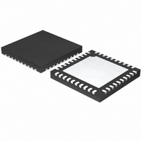
MAX8686ETL+ Maxim Integrated Products, MAX8686ETL+ Datasheet - Page 11

MAX8686ETL+
Manufacturer Part Number
MAX8686ETL+
Description
IC BUCK SYNC ADJ 25A 40TQFN
Manufacturer
Maxim Integrated Products
Type
Step-Down (Buck)r
Datasheet
1.MAX8686ETL.pdf
(23 pages)
Specifications of MAX8686ETL+
Internal Switch(s)
Yes
Synchronous Rectifier
Yes
Number Of Outputs
1
Voltage - Output
0.7 ~ 5.5 V
Current - Output
25A
Frequency - Switching
300kHz ~ 1MHz
Voltage - Input
4.5 ~ 20 V
Operating Temperature
-40°C ~ 85°C
Mounting Type
Surface Mount
Package / Case
40-TQFN Exposed Pad
Power - Output
4W
Lead Free Status / RoHS Status
Lead free / RoHS Compliant
The MAX8686 step-down regulator uses a PWM, cur-
rent-mode control scheme. An internal transconduc-
tance amplifier establishes an integrated error voltage.
The heart of the PWM controller is a PWM comparator
that compares the integrated voltage-feedback signal
against the amplified current-sense signal plus an
adjustable slope-compensation ramp, which is
summed with the current signal to ensure stability. At
each rising edge of the internal clock, the internal high-
side MOSFET turns on until the PWM comparator trips
or the maximum duty cycle is reached. During this on-
time, current ramps up through the inductor, storing
energy in the inductor while sourcing current to the
output. The current-mode feedback system regulates the
peak inductor current as a function of the output-voltage
error signal. The circuit acts as a switch-mode transcon-
ductance amplifier and pushes an output LC filter pole
normally found in a voltage-mode PWM to a higher fre-
quency. See the Functional Diagram .
During the second half of the cycle, the internal high-side
MOSFET turns off and the internal low-side MOSFET
turns on. The inductor releases the stored energy as the
current ramps down, providing current to the load. The
output capacitor stores charge when the inductor cur-
rent exceeds the required load current and discharges
when the inductor current is lower, smoothing the volt-
age across the load. Under soft-overload conditions,
when the peak inductor current exceeds the selected
current limit (see the Current-Limit Circuit section), the
high-side MOSFET is turned off immediately and the
low-side MOSFET is turned on and remains on to let the
inductor current ramp down until the next clock cycle.
Under severe-overload or short-circuit conditions, the
foldback/hiccup current limit is enabled to reduce
power dissipation.
The MAX8686 operates in a forced-PWM mode. The
converter maintains a constant switching frequency,
regardless of load, to allow for easier filtering of the
switching noise.
The MAX8686 contains an internal LDO regulator that
provides a 5.4V supply for the MOSFET gate drivers.
Connect at least a 1μF ceramic capacitor from VL to
DC-DC Converter Delivers Up to 25A Per Phase
DC-DC Converter Control Architecture
Internal Linear Regulator (VL)
______________________________________________________________________________________
Detailed Description
Single/Multiphase, Step-Down,
RTN. VL also provides power to the internal analog cir-
cuit through AVL. Connect an RC lowpass filter (R =
10Ω, C = 0.22μF) from VL to AVL.
When AVL drops below 4.03V, the MAX8686 assumes
that the supply voltage is too low to make valid deci-
sions, so the undervoltage-lockout (UVLO) circuitry
inhibits switching and turns off both power MOSFETs.
When AVL rises above 4.35V, the regulator enters the
startup sequence and then resumes normal operation.
When operating in a multiphase configuration, the AVL
of all the devices must exceed the UVLO threshold
before any switching begins. This is achieved through
the shared ILIM pin, which is pulled low in UVLO.
The internal soft-start circuitry gradually ramps up the
reference voltage in order to control the rate of rise of
the output voltage and reduce input surge currents dur-
ing startup. The soft-start time is determined by the
value of the capacitor from SS to GND and is approxi-
mately equal to 50ms per microfarad of the capacitor.
In addition, the MAX8686 features monotonic output-
voltage rise (prebias); therefore, both power MOSFETs
are kept off if the voltage between the remote sense
input (RS+, RS-) is higher than the voltage at REFIN.
This allows the MAX8686 to start up into a prebiased
output without pulling the output voltage down.
Before the MAX8686 can begin the soft-start and
power-up sequence, the following conditions must be
met: AVL exceeds the 4.35V UVLO threshold, EN is at
logic-high, and the thermal limit is not exceeded.
The reference voltage REFO can be used to set the out-
put voltage by scaling this voltage down with a resistive
divider and using it as the input voltage to the reference
input, REFIN. The 3.3V reference voltage is 1% accurate
over temperature and can source up to 20μA.
The reference input REFIN allows the reference value of
the device to be set by an external reference. In most
applications, the 3.3V voltage with 1% accuracy from
the PHASE/REFO pin should be used as the reference.
This can be achieved by dividing the 3.3V voltage to
the desired output voltage.
Startup, Soft-Start, and Prebias Operation
(PHASE/REFO)/Reference Input (REFIN)
Undervoltage Lockout
Reference Output
11


