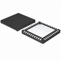
MAX8686ETL+ Maxim Integrated Products, MAX8686ETL+ Datasheet - Page 2

MAX8686ETL+
Manufacturer Part Number
MAX8686ETL+
Description
IC BUCK SYNC ADJ 25A 40TQFN
Manufacturer
Maxim Integrated Products
Type
Step-Down (Buck)r
Datasheet
1.MAX8686ETL.pdf
(23 pages)
Specifications of MAX8686ETL+
Internal Switch(s)
Yes
Synchronous Rectifier
Yes
Number Of Outputs
1
Voltage - Output
0.7 ~ 5.5 V
Current - Output
25A
Frequency - Switching
300kHz ~ 1MHz
Voltage - Input
4.5 ~ 20 V
Operating Temperature
-40°C ~ 85°C
Mounting Type
Surface Mount
Package / Case
40-TQFN Exposed Pad
Power - Output
4W
Lead Free Status / RoHS Status
Lead free / RoHS Compliant
Single/Multiphase, Step-Down,
DC-DC Converter Delivers Up to 25A Per Phase
ABSOLUTE MAXIMUM RATINGS
IN, INA to PGND.....................................................-0.3V to +22V
BST, DH to LX...........................................................-0.3V to +6V
BST to PGND..........................................................-0.3V to +28V
LX to PGND...........................-0.3V to (V
BST to VL................................................................-0.3V to +22V
AVL to GND.................................................-0.3V to (V
COMP, ILIM, FREQ, PHASE/REFO, RS+, RS-, POK, REFIN,
VL to PGND ..............................................................-0.3V to +6V
EN/SLOPE to GND ...................................................-0.3V to +6V
RTN to PGND to GND to GFREQ ..........................-0.3V to +0.3V
IN Continuous Current.....................................................20A
ELECTRICAL CHARACTERISTICS
(V
C
Note 1: Package thermal resistances were obtained using the method described in JEDEC specification JESD51-7, using a four-layer
Stresses beyond those listed under “Absolute Maximum Ratings” may cause permanent damage to the device. These are stress ratings only, and functional
operation of the device at these or any other conditions beyond those indicated in the operational sections of the specifications is not implied. Exposure to
absolute maximum rating conditions for extended periods may affect device reliability.
2
GENERAL
Operating Input-Voltage Range
Operating Input-Voltage Range
IN/INA Shutdown Supply Current
IN/INA Quiescent Supply Current
AVL Undervoltage Lockout Trip
Level
VL Output Voltage
SOFT-START (SS)
SS Shutdown Resistance
SS Soft-Start Current
PHASE COMPARATOR AND REFERENCE (PHASE/REFO)
Reference Output Voltage
PHASE Comparator Offset
REFIN INPUT
REFIN Input Bias Current
REFIN Input Voltage Range
AVL
IN
CS+, CS- to GND ..................................-0.3V to (V
_______________________________________________________________________________________
= V
= 0.22μF, C
INA
board. For detailed information on package thermal considerations see www.maxim-ic.com/thermal-tutorial.
PARAMETER
= 12V, VL = AVL, V
FREQ
= 270pF, T
REFIN
A
= +25°C, unless otherwise noted.) (Note 2)
= 1V, V
V
V
V
V
V
T
Rising, T
Falling
6V ≤ V
T
V
V
Measured at PHASE/REFO (master mode),
T
V
T
V
A
A
A
A
INA
IN
EN/SLOPE
IN
RS+
EN/SLOPE
SS
RS-
REFIN
IN
= -40°C to +85°C
= -40°C to +85°C
= -40°C to +85°C
= -40°C to +85°C
= V
= V
= 0.4V and 1.1V, T
= V
= V
+ 0.3V) (-2V for 50ns)
= 1.1V, no switching; V
RS+
IN
INA
INA
= 0.7V or 3.3V
AVL
IN
A
= V
- V
= -40°C to +85°C
, T
= V
= 0V,
= 20V
= 0V (master mode)
INA
(slave mode), V
RS-
A
VL
AVL
= -40°C to +85°C
≤ 20V, 1mA ≤ I
VL
= 1V, V
= V
+ 0.3V)
+ 0.3V)
AVL
CONDITIONS
RMS
A
RS-
, T
= -40°C to +85°C
A
= 0V, V
PHASE
IN
= -40°C to +85°C
VL
= V
LX Continuous Current ....................................................25A
Continuous Power Dissipation (T
θ
θ
Operating Temperature Range ...........................-40°C to +85°C
Junction Temperature ......................................................+150°C
Storage Temperature Range .............................-65°C to +150°C
Lead Temperature (soldering, 10s) .................................+300°C
Soldering Temperature (reflow) .......................................+260°C
≤ 30mA,
JC
JT
EN/SLOPE
INA
= 0.3V and 2.5V,
40-Pin TQFN (derate 50mW/°C above +70°C) ..........4000mW
(Note 1) ......................................................................3.5°C/W
T
T
(thermal resistance from junction to top) (Note 1) ...3.9°C/W
(thermal resistance from junction to exposed pad)
A
A
= 20V,
= +25°C
= +85°C
= 1.25V, V
CS+
= V
3.267
-500
MIN
4.2
5.2
-20
4.5
19
CS-
6
0
= 1V, R
A
= +70°C) (Note 1)
3.300
TYP
4.35
4.03
450
500
5.5
5.4
20
25
ILIM
= 122kΩ, C
3.333
MAX
+500
4.45
100
+20
5.5
6.6
5.5
3.3
20
31
VL
UNITS
mA
mV
= 1μF,
μA
μA
nA
Ω
V
V
V
V
V
V
RMS


