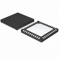
MAX8686ETL+ Maxim Integrated Products, MAX8686ETL+ Datasheet - Page 12

MAX8686ETL+
Manufacturer Part Number
MAX8686ETL+
Description
IC BUCK SYNC ADJ 25A 40TQFN
Manufacturer
Maxim Integrated Products
Type
Step-Down (Buck)r
Datasheet
1.MAX8686ETL.pdf
(23 pages)
Specifications of MAX8686ETL+
Internal Switch(s)
Yes
Synchronous Rectifier
Yes
Number Of Outputs
1
Voltage - Output
0.7 ~ 5.5 V
Current - Output
25A
Frequency - Switching
300kHz ~ 1MHz
Voltage - Input
4.5 ~ 20 V
Operating Temperature
-40°C ~ 85°C
Mounting Type
Surface Mount
Package / Case
40-TQFN Exposed Pad
Power - Output
4W
Lead Free Status / RoHS Status
Lead free / RoHS Compliant
Single/Multiphase, Step-Down,
DC-DC Converter Delivers Up to 25A Per Phase
For using an external reference on REFIN, SS needs to
be tied to REFIN either directly or indirectly through a
resistor for soft-start. For REFIN voltage lower than
1.25V, connect a resistor between SS and REFIN such
that the voltage drop across the resistor due to the soft-
start current (31μA max) coming out of SS, causing the
final SS voltage to be at least 1.25V (see Figure 1a).
The external reference should be able to sink at least
31μA. Calculate R
where V
In a multiphase converter, only REFIN of the master
device is connected to a reference voltage, and the
REFIN of all slave devices should be tied to GND.
The REFIN also allows for coincident voltage tracking of
multiple converters during power-up/power-down by
applying the same voltage on REFIN of the master
device in each converter.
An internal 10μA current source pulls the EN/SLOPE
input high. The device shuts down when the voltage at
the EN/SLOPE falls below 0.7V. By connecting an
open-drain or open-collector switch to the EN/SLOPE,
this pin can be used to enable/disable a single-phase
or multiphase converter system.
A separate system signal can be used to shed some
phases of the converter at light load to eliminate all the
power loss from these phases and thus improve the sys-
tem efficiency. The phase shedding signal is connected
to the EN/SLOPE pins of the slave devices to be shed.
Figure 1a. Using an External Reference
12
______________________________________________________________________________________
Slope Compensation Input (EN/SLOPE)
EXT
is the external reference voltage.
MAX8686
R
REFIN
REFIN
Enable, Phase Shedding, and
REFIN
as follows:
=
SS
1 25
.
19
−
μA
V
EXT
R
REFIN
V
EXT
The right timing of the phase shedding signal from the
system is critical for the safe operation of the multiphase
converter. Only after the load current drops below a cer-
tain level, should the phase shedding signal become
high. When the open-drain or open-collector switch is
logic-low, it shuts down the slave phases connected to
the switch to reduce power loss. Before the load current
increases to a certain level, the phase shedding signal
should become logic-high to release the EN/SLOPE of
these slave devices, thus turning these phases back on
again to prepare for the higher load current. A minimum
load of 2A per phase in the remaining phases is
required for the shedded phase(s) to turn on.
The transfer function of the power stage is different with a
different number of phases. As the number of phases
increases, the power stage gain increases. The compen-
sation network should be designed such that the convert-
er is always stable with the maximum number of phases.
The EN/SLOPE input is also used to set the slope com-
pensation ramp voltage by connecting a resistor from this
input to GND. The slope compensation is used to stabi-
lize the converters when the duty cycle is more than 40%.
A flying capacitor between BST and LX generates the
gate-drive voltage for the internal high-side n-channel
MOSFET. When the low-side MOSFET is turned on, the
capacitor is charged by VL to 5.4V minus the drop
across the internal boost switch. When the low-side
MOSFET is turned off, the stored voltage of the capaci-
tor is stacked above LX to provide the necessary turn-
on voltage (V
switch between BST and the internal high-side MOSFET’s
gate closes to turn the MOSFET on.
The current-sense circuit amplifies the differential current-
sense voltage (V
signal and the internal-slope-compensation signal are
summed (V
parator’s inverting input. The high-side MOSFET is turned
on by the clock in the device and is shut off when V
exceeds the error-amplifier output voltage (V
the noninverting input of the PWM comparator. The dif-
ferential current sense is also used to provide peak
inductor current limiting. The limit can be set by adjust-
ing the analog current-limit input (ILIM).
The current-sense amplifier is used to measure the cur-
rent across the inductor by connecting to the inductor
through an RC network for lossless current sensing or
connecting to a current-sense resistor for higher accu-
racy. The input common-mode voltage range of the
current-sense amplifier is from 0 to 5.5V.
High-Side Gate-Drive Supply (BST)
SUM
GS
) together and fed into the PWM com-
) for the high-side MOSFET. An internal
CS+
- V
CS-
Current-Sense Amplifier
). This amplified current-sense
COMP
SUM
) at


