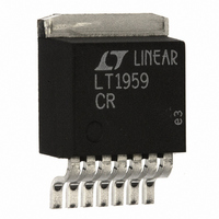
LT1959CR#TRPBF Linear Technology, LT1959CR#TRPBF Datasheet - Page 13

LT1959CR#TRPBF
Manufacturer Part Number
LT1959CR#TRPBF
Description
IC SW REG STEP-DWN 500KHZ 7-DD
Manufacturer
Linear Technology
Type
Step-Down (Buck)r
Datasheet
1.LT1959CS8PBF.pdf
(24 pages)
Specifications of LT1959CR#TRPBF
Internal Switch(s)
Yes
Synchronous Rectifier
No
Number Of Outputs
1
Voltage - Output
1.21 ~ 38 V
Current - Output
4.5A
Frequency - Switching
500kHz
Voltage - Input
4.3 ~ 15 V
Operating Temperature
0°C ~ 125°C
Mounting Type
Surface Mount
Package / Case
D²Pak, TO-263 (7 leads + tab)
Dc To Dc Converter Type
Step Down
Pin Count
7 +Tab
Input Voltage
16V
Output Voltage
1.21 to 2.42V
Switching Freq
540kHz
Output Current
8.5A
Package Type
DDPAK
Output Type
Adjustable
Switching Regulator
Yes
Line Regulation
0.03%/V
Mounting
Surface Mount
Input Voltage (min)
4V
Operating Temperature Classification
Commercial
Lead Free Status / RoHS Status
Lead free / RoHS Compliant
Power - Output
-
Lead Free Status / Rohs Status
Compliant
Available stocks
Company
Part Number
Manufacturer
Quantity
Price
APPLICATIONS
and does not fall to less than 1/3 of nominal output voltage,
foldback will not take effect. With the overloaded condi-
tion, output current will increase to a typical value of 5.7A,
determined by peak switch current limit of 6A. With
V
This is safe for short periods of time, but it would be
prudent to check with the diode manufacturer if continu-
ous operation under these conditions must be tolerated.
BOOST PIN CONSIDERATIONS
For most applications, the boost components are a 0.27 F
capacitor and a 1N914 or 1N4148 diode. The anode is
connected to the regulated output voltage and this gener-
ates a voltage across the boost capacitor nearly identical
to the regulated output. In certain applications, the anode
may instead be connected to the unregulated input volt-
age. This could be necessary if the regulated output
voltage is very low (< 3V) or if the input voltage is less than
5V. Efficiency is not affected by the capacitor value, but the
capacitor should have an ESR of less than 1 to ensure
that it can be recharged fully under the worst-case condi-
tion of minimum input voltage. Almost any type of film or
ceramic capacitor will work fine.
For nearly all applications, a 0.27 F boost capacitor works
just fine, but for the curious, more details are provided
here. The size of the boost capacitor is determined by
switch drive current requirements. During switch on time,
drain current on the capacitor is approximately I
peak load current of 4.25A, this gives a total drain of 85mA.
Capacitor ripple voltage is equal to the product of on time
and drain current divided by capacitor value;
less than 0.6V (a slightly arbitrary number) at the worst-
case condition of t
0.27 F. Boost capacitor ripple voltage is not a critical
parameter, but if the minimum voltage across the capaci-
tor drops to less than 3V, the power switch may not
saturate fully and efficiency will drop. An approximate
formula for absolute minimum capacitor value is:
IN
V = (t
I
D AVG
= 15V, V
ON
)(85mA/C). To keep capacitor ripple voltage to
OUT
5 7 15 4
.
= 4V (5V overloaded) and I
15
ON
U
= 1.8 s, the capacitor needs to be
INFORMATION
U
4 18
.
A
W
OUT
OUT
U
= 5.7A:
/ 50. At
f = Switching frequency
V
V
This formula can yield capacitor values substantially less
than 0.27 F, but it should be used with caution since it
does not take into account secondary factors such as
capacitor series resistance, capacitance shift with tem-
perature and output overload.
SHUTDOWN FUNCTION AND UNDERVOLTAGE
LOCKOUT
Figure 4 shows how to add undervoltage lockout (UVLO)
to the LT1959. Typically, ULVO is used in situations where
the input supply is current limited , or has a relatively high
source resistance. A switching regulator draws constant
power from the source, so source current increases as
source voltage drops. This looks like a negative resistance
load to the source and can cause the source to current limit
or latch low under low source voltage conditions. ULVO
prevents the regulator from operating at source voltages
where these problems might occur.
Threshold voltage for lockout is about 2.38V. A 3.5 A bias
current flows out of the pin at threshold. This internally
generated current is used to force a default high state on
the shutdown pin if the pin is left open. When low shut-
down current is not an issue, the error due to this current
can be minimized by making R
current is an issue, R
due to initial bias current and changes with temperature
should be considered.
V
OUT
IN
IN
R
R
C
= Minimum input voltage
= Minimum input voltage
MIN
LO
HI
= Regulated output voltage
2 38
10
R
k
I
LO
OUT
to 100k 25k suggested
V R
f V
V
IN
/
50
OUT
LO
LO
2 38
3 5
V
can be raised to 100k, but the error
OUT
2 8
V
.
A
/
V
V
LO
IN
10k or less. If shutdown
LT1959
13


