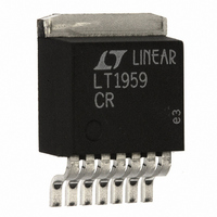
LT1959CR#TRPBF Linear Technology, LT1959CR#TRPBF Datasheet - Page 14

LT1959CR#TRPBF
Manufacturer Part Number
LT1959CR#TRPBF
Description
IC SW REG STEP-DWN 500KHZ 7-DD
Manufacturer
Linear Technology
Type
Step-Down (Buck)r
Datasheet
1.LT1959CS8PBF.pdf
(24 pages)
Specifications of LT1959CR#TRPBF
Internal Switch(s)
Yes
Synchronous Rectifier
No
Number Of Outputs
1
Voltage - Output
1.21 ~ 38 V
Current - Output
4.5A
Frequency - Switching
500kHz
Voltage - Input
4.3 ~ 15 V
Operating Temperature
0°C ~ 125°C
Mounting Type
Surface Mount
Package / Case
D²Pak, TO-263 (7 leads + tab)
Dc To Dc Converter Type
Step Down
Pin Count
7 +Tab
Input Voltage
16V
Output Voltage
1.21 to 2.42V
Switching Freq
540kHz
Output Current
8.5A
Package Type
DDPAK
Output Type
Adjustable
Switching Regulator
Yes
Line Regulation
0.03%/V
Mounting
Surface Mount
Input Voltage (min)
4V
Operating Temperature Classification
Commercial
Lead Free Status / RoHS Status
Lead free / RoHS Compliant
Power - Output
-
Lead Free Status / Rohs Status
Compliant
Available stocks
Company
Part Number
Manufacturer
Quantity
Price
LT1959
APPLICATIONS
Keep the connections from the resistors to the shutdown
pin short and make sure that interplane or surface capaci-
tance to the switching nodes are minimized. If high
resistor values are used, the shutdown pin should be
bypassed with a 1000pF capacitor to prevent coupling
problems from the switch node. If hysteresis is desired in
the undervoltage lockout point, a resistor R
added to the output node. Resistor values can be calcu-
lated from:
25k suggested for R
V
Example: output voltage is 5V, switching is to stop if input
voltage drops below 6V and should not restart unless
input rises back to 7.5V. V is therefore 1.5V and V
Let R
14
IN
V = Hysteresis in input voltage level
R
R
= Input voltage at which switching stops as input
HI
FB
LO
voltage descends to trip level
= 25k.
R
R
LO IN
HI
V
V
INPUT
OUT
2 38
2 38
U
LO
C1
V
INFORMATION
R
U
V V
2 3 5
R
R
LO
HI
OUT
A
W
IN
SHDN
LT1959
1
V
Figure 4. Undervoltage Lockout
FB
3.5 A
U
IN
can be
2.38V
= 6V.
0.4V
GND
R
FB
SWITCH NODE CONSIDERATIONS
For maximum efficiency, switch rise and fall times are
made as short as possible. To prevent radiation and high
frequency resonance problems, proper layout of the com-
ponents connected to the switch node is essential. B field
(magnetic) radiation is minimized by keeping catch diode,
switch pin, and input bypass capacitor leads as short as
possible. E field radiation is kept low by minimizing the
length and area of all traces connected to the switch pin
and BOOST pin. A ground plane should always be used
under the switcher circuitry to prevent interplane cou-
pling. A suggested layout for the critical components is
shown in Figure 5. Note that the feedback resistors and
compensation components are kept as far as possible
R
R
HI
FB
25 5 2
25 6 2 38 1 5 5 1
48 5 1 5
2 29
k
k
k
.
LOCKOUT
TOTAL
SHUTDOWN
2 38 25 3 5
.
/ .
.
.
V
48
SW
160
k
. /
k
k
.
A
+
1 5
.
OUTPUT
1959 F04


