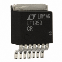
LT1959CR#TRPBF Linear Technology, LT1959CR#TRPBF Datasheet - Page 8

LT1959CR#TRPBF
Manufacturer Part Number
LT1959CR#TRPBF
Description
IC SW REG STEP-DWN 500KHZ 7-DD
Manufacturer
Linear Technology
Type
Step-Down (Buck)r
Datasheet
1.LT1959CS8PBF.pdf
(24 pages)
Specifications of LT1959CR#TRPBF
Internal Switch(s)
Yes
Synchronous Rectifier
No
Number Of Outputs
1
Voltage - Output
1.21 ~ 38 V
Current - Output
4.5A
Frequency - Switching
500kHz
Voltage - Input
4.3 ~ 15 V
Operating Temperature
0°C ~ 125°C
Mounting Type
Surface Mount
Package / Case
D²Pak, TO-263 (7 leads + tab)
Dc To Dc Converter Type
Step Down
Pin Count
7 +Tab
Input Voltage
16V
Output Voltage
1.21 to 2.42V
Switching Freq
540kHz
Output Current
8.5A
Package Type
DDPAK
Output Type
Adjustable
Switching Regulator
Yes
Line Regulation
0.03%/V
Mounting
Surface Mount
Input Voltage (min)
4V
Operating Temperature Classification
Commercial
Lead Free Status / RoHS Status
Lead free / RoHS Compliant
Power - Output
-
Lead Free Status / Rohs Status
Compliant
Available stocks
Company
Part Number
Manufacturer
Quantity
Price
LT1959
APPLICATIONS
FEEDBACK PIN FUNCTIONS
The feedback (FB) pin on the LT1959 is used to set output
voltage and provide several overload protection features.
The first part of this section deals with selecting resistors
to set output voltage and the remaining part talks about
foldback frequency and current limiting created by the FB
pin. Please read both parts before committing to a final
design.
The suggested value for the output divider resistor (see
Figure 2) from FB to ground (R2) is 2.5k or less, and a
formula for R1 is shown below. The output voltage error
caused by ignoring the input bias current on the FB pin is
less than 0.1% with R2 = 2.5k. Please read the following
if divider resistors are increased above the suggested
values.
8
LT1959
V
C
Q2
R
1
GND
AMPLIFIER
Figure 2. Frequency and Current Limit Foldback
R V
ERROR
2
R5
TO FREQUENCY
5k
TO SYNC CIRCUIT
OUT
SHIFTING
1 21
+
–
.
1V
U
1.21V
1 21
.
Q1
INFORMATION
R3
U
1k
R4
1k
W
V
SW
FB
R1
R2
2.5k
U
+
1959 F02
OUTPUT
5V
More Than Just Voltage Feedback
The feedback pin is used for more than just output voltage
sensing. It also reduces switching frequency and current
limit when output voltage is very low (see the Frequency
Foldback graph in Typical Performance Characteristics).
This is done to control power dissipation in both the IC and
in the external diode and inductor during short-circuit
conditions. A shorted output requires the switching regu-
lator to operate at very low duty cycles, and the average
current through the diode and inductor is equal to the
short-circuit current limit of the switch (typically 6A for the
LT1959, folding back to less than 3A). Minimum switch on
time limitations would prevent the switcher from attaining
a sufficiently low duty cycle if switching frequency were
maintained at 500kHz, so frequency is reduced by about
5:1 when the feedback pin voltage drops below 0.5V (see
Frequency Foldback graph). This does not affect operation
with normal load conditions; one simply sees a gear shift
in switching frequency during start-up as the output
voltage rises.
In addition to lower switching frequency, the LT1959 also
operates at lower switch current limit when the feedback
pin voltage drops below 0.8V. Q2 in Figure 2 performs this
function by clamping the V
normal 2.1V upper clamp level. This foldback current limit
greatly reduces power dissipation in the IC, diode and
inductor during short-circuit conditions. External synchro-
nization is also disabled to prevent interference with
foldback operation. Again, it is nearly transparent to the
user under normal load conditions. The only loads that may
be affected are current source loads which maintain full
load current with output voltage less than 50% of final value.
In these rare situations the feedback pin can be clamped
above 0.75V with an external diode to defeat foldback cur-
rent limit. Caution: clamping the feedback pin means that
frequency shifting will also be defeated, so a combination
of high input voltage and dead shorted output may cause
the LT1959 to lose control of current limit.
C
pin to a voltage less than its


