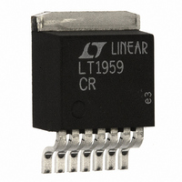
LT1959CR#TRPBF Linear Technology, LT1959CR#TRPBF Datasheet - Page 20

LT1959CR#TRPBF
Manufacturer Part Number
LT1959CR#TRPBF
Description
IC SW REG STEP-DWN 500KHZ 7-DD
Manufacturer
Linear Technology
Type
Step-Down (Buck)r
Datasheet
1.LT1959CS8PBF.pdf
(24 pages)
Specifications of LT1959CR#TRPBF
Internal Switch(s)
Yes
Synchronous Rectifier
No
Number Of Outputs
1
Voltage - Output
1.21 ~ 38 V
Current - Output
4.5A
Frequency - Switching
500kHz
Voltage - Input
4.3 ~ 15 V
Operating Temperature
0°C ~ 125°C
Mounting Type
Surface Mount
Package / Case
D²Pak, TO-263 (7 leads + tab)
Dc To Dc Converter Type
Step Down
Pin Count
7 +Tab
Input Voltage
16V
Output Voltage
1.21 to 2.42V
Switching Freq
540kHz
Output Current
8.5A
Package Type
DDPAK
Output Type
Adjustable
Switching Regulator
Yes
Line Regulation
0.03%/V
Mounting
Surface Mount
Input Voltage (min)
4V
Operating Temperature Classification
Commercial
Lead Free Status / RoHS Status
Lead free / RoHS Compliant
Power - Output
-
Lead Free Status / Rohs Status
Compliant
Available stocks
Company
Part Number
Manufacturer
Quantity
Price
LT1959
APPLICATIONS
G
G
ESR = Output capacitor ESR
1.21 = Reference voltage
With V
would yield zero gain margin, so this represents an upper
limit. There is a second limitation however which has
nothing to do with theoretical small signal dynamics. This
resistor sets high frequency gain of the error amplifier,
including the gain at the switching frequency. If switching
frequency gain is high enough, output ripple voltage will
appear at the V
proper operation of the regulator. In the marginal case,
subharmonic switching occurs, as evidenced by alternat-
ing pulse widths seen at the switch node. In more severe
cases, the regulator squeals or hisses audibly even though
the output voltage is still roughly correct. None of this will
show on a theoretical Bode plot because Bode is an
amplitude insensitive analysis. Tests have shown that if
ripple voltage on the V
LT1959 will be well behaved . The formula below will give
an estimate of V
loop, assuming that R
of C
G
If a computer simulation of the LT1959 showed that a
series compensation resistor of 6k gave best overall loop
response, with adequate gain margin, the resulting V
ripple voltage with V
L = 10 H, would be:
This ripple voltage is high enough to possibly create
subharmonic switching. In most situations a compromise
value (< 2k in this case) for the resistor gives acceptable
phase margin and no subharmonic problems. In other
20
V
MP
MA
MA
C RIPPLE
V
C
C RIPPLE
= Transconductance of power stage = 5.3A/V
= Error amplifier transconductance = 2(10
= Error amplifier transconductance (2000 Mho)
at 500kHz.
OUT
= 5V and ESR = 0.03 , a value of 6.5k for R
6
C
k
C
pin with enough amplitude to muck up
R
10 10 10
ripple voltage when R
C
2 10
U
•
IN
C
C
G
is large compared to the reactance
is held to less than 100mV
MA
= 10V, V
INFORMATION
•
3
U
V
10 5 0 1 1 21
IN
6
V
IN
OUT
500 10
V
L f
W
OUT
= 5V, ESR = 0.1 ,
•
.
C
3
ESR
is added to the
.
U
–3
1 21
.
0 144
)
P-P
.
C
, the
pin
V
C
cases, the resistor may have to be larger to get acceptable
phase response, and some means must be used to control
ripple voltage at the V
is to add a capacitor (C
on the V
set at one-fifth of switching frequency so that it provides
significant attenuation of switching ripple, but does not
add unacceptable phase shift at loop unity-gain frequency.
With R
How Do I Test Loop Stability?
The “standard” compensation for LT1959 is a 1.5nF
capacitor for C
work for most applications, the “optimum” value for loop
compensation components depends, to various extent, on
parameters which are not well controlled. These include
inductor value ( 30% due to production tolerance, load
current and ripple current variations), output capacitance
( 20% to 50% due to production tolerance, tempera-
ture, aging and changes at the load), output capacitor ESR
( 200% due to production tolerance, temperature and
aging), and finally, DC input voltage and output load
current . This makes it important for the designer to check
out the final design to ensure that it is “robust” and tolerant
of all these variations.
I check switching regulator loop stability by pulse loading
the regulator output while observing transient response at
the output, using the circuit shown in Figure 13. The
regulator loop is “hit” with a small transient AC load
current at a relatively low frequency, 50Hz to 1kHz. This
causes the output to jump a few millivolts, then settle back
to the original value, as shown in Figure 14. A well behaved
loop will settle back cleanly, whereas a loop with poor
phase or gain margin will “ring” as it settles. The number
of rings indicates the degree of stability, and the frequency
of the ringing shows the approximate unity-gain fre-
quency of the loop. Amplitude of the signal is not particu-
larly important, as long as the amplitude is not so high that
the loop behaves nonlinearly.
C
F
C
C
= 6k,
pin. Pole frequency for this capacitor is typically
2
5
C
f R
, with R
C
C
F
) in parallel with the R
C
pin. The suggested way to do this
2 500 10
= 0. While this compensation will
5
3
6
k
C
/C
275
C
network
pF


