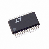
LTC3728LEGN-1#PBF Linear Technology, LTC3728LEGN-1#PBF Datasheet - Page 18

LTC3728LEGN-1#PBF
Manufacturer Part Number
LTC3728LEGN-1#PBF
Description
IC REG SYNC DUAL 28-SSOP
Manufacturer
Linear Technology
Series
PolyPhase®r
Type
Step-Down (Buck)r
Datasheet
1.LTC3728LEGN-1PBF.pdf
(32 pages)
Specifications of LTC3728LEGN-1#PBF
Internal Switch(s)
No
Synchronous Rectifier
Yes
Number Of Outputs
2
Voltage - Output
0.8 ~ 7 V
Current - Output
3A
Frequency - Switching
250kHz ~ 550kHz
Voltage - Input
4.5 ~ 28 V
Operating Temperature
-40°C ~ 85°C
Mounting Type
Surface Mount
Package / Case
28-SSOP
Lead Free Status / RoHS Status
Lead free / RoHS Compliant
Power - Output
-
Available stocks
Company
Part Number
Manufacturer
Quantity
Price
APPLICATIONS INFORMATION
LTC3728L-1
2. EXTV
connection for a 5V regulator and provides the highest
effi ciency.
3. EXTV
supply is available in the 5V to 7V range, it may be used to
power EXTV
gate drive requirements.
4. EXTV
For 3.3V and other low voltage regulators, effi ciency gains
can still be realized by connecting EXTV
derived voltage that has been boosted to greater than 4.7V.
This can be done with either the inductive boost winding
as shown in Figure 6a or the capacitive charge pump
shown in Figure 6b. The charge pump has the advantage
of simple magnetics.
Topside MOSFET Driver Supply (C
External bootstrap capacitors C
pins supply the gate drive voltages for the topside MOSFETs.
Capacitor C
external diode D
When one of the topside MOSFETs is to be turned on,
the driver places the C
of the desired MOSFET. This enhances the MOSFET and
turns on the topside switch. The switch node voltage, SW,
rises to V
MOSFET on, the boost voltage is above the input supply:
18
R6
R5
Figure 6a. Secondary Output Loop & EXTV
OPTIONAL EXTV
CONNECTION
5V < V
EXTV
FCB
SGND
CC
CC
CC
IN
LTC3728L-1
Connected to an Output-Derived Boost Network.
Connected to an External supply. If an external
CC
Connected directly to V
SEC
B
CC
and the BOOST pin follows. With the topside
in the functional diagram is charged through
< 7V
providing it is compatible with the MOSFET
B
PGND
CC
TG1
BG1
SW
from INTV
V
IN
N-CH
N-CH
B
voltage across the gate-source
V
IN
+
CC
B
C
when the SW pin is low.
IN
connected to the BOOST
BAT 85
1:N
T1
OUT
B
, D
. This is the normal
B
R
CC
)
CC
SENSE
3728L1 F06a
Connection
to an output-
V
SEC
+
+
1μF
C
V
OUT
OUT
V
C
of the topside MOSFET(s). The reverse breakdown of the
external Schottky diode must be greater than V
When adjusting the gate drive level, the fi nal arbiter is the
total input current for the regulator. If a change is made
and the input current decreases, then the effi ciency has
improved. If there is no change in input current, then there
is no change in effi ciency.
Output Voltage
The output voltages are each set by an external feedback
resistive divider carefully placed across the output capacitor.
The resultant feedback signal is compared with the internal
precision 0.800V voltage reference by the error amplifi er.
The output voltage is given by the equation:
where R1 and R2 are defi ned in Figure 2.
SENSE
The common mode input range of the current comparator
sense pins is from 0V to (1.1)INTV
operation is guaranteed throughout this range allowing
output voltage setting from 0.8V to 7.7V, depending upon
the voltage applied to EXTV
BOOST
B
needs to be 100 times that of the total input capacitance
V
OUT
EXTV
+
LTC3728L-1
= V
CC
/SENSE
Figure 6b. Capacitive Charge Pump for EXTV
= 0.8V 1+
IN
+ V
PGND
TG1
BG1
SW
V
–
C
IN
IN
INTVCC
Pins
+
N-CH
N-CH
R2
R1
V
. The value of the boost capacitor
IN
BAT85
CC
. A differential NPN input
L1
VN2222LL
CC
R
. Continuous linear
SENSE
0.22μF
+
+
CC
BAT85
BAT85
IN(MAX)
1μF
C
3728L1 F06b
V
OUT
OUT
3728l1fc
.


