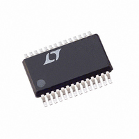
LTC3728LEGN-1#PBF Linear Technology, LTC3728LEGN-1#PBF Datasheet - Page 21

LTC3728LEGN-1#PBF
Manufacturer Part Number
LTC3728LEGN-1#PBF
Description
IC REG SYNC DUAL 28-SSOP
Manufacturer
Linear Technology
Series
PolyPhase®r
Type
Step-Down (Buck)r
Datasheet
1.LTC3728LEGN-1PBF.pdf
(32 pages)
Specifications of LTC3728LEGN-1#PBF
Internal Switch(s)
No
Synchronous Rectifier
Yes
Number Of Outputs
2
Voltage - Output
0.8 ~ 7 V
Current - Output
3A
Frequency - Switching
250kHz ~ 550kHz
Voltage - Input
4.5 ~ 28 V
Operating Temperature
-40°C ~ 85°C
Mounting Type
Surface Mount
Package / Case
28-SSOP
Lead Free Status / RoHS Status
Lead free / RoHS Compliant
Power - Output
-
Available stocks
Company
Part Number
Manufacturer
Quantity
Price
APPLICATIONS INFORMATION
pulling up the PLLFLTR pin. When the external frequency is
less than f
the PLLFLTR pin. If the external and internal frequencies
are the same but exhibit a phase difference, the current
sources turn on for an amount of time corresponding to
the phase difference. Thus the voltage on the PLLFLTR pin
is adjusted until the phase and frequency of the external
and internal oscillators are identical. At this stable operat-
ing point the phase comparator output is open and the
fi lter capacitor C
must be driven from a low impedance source such as a
logic gate located close to the pin. When using multiple
ICs for a phase-locked system, the PLLFLTR pin of the
master oscillator should be biased at a voltage that will
guarantee the slave oscillator(s) ability to lock onto the
master’s frequency. A DC voltage of 0.7V to 1.7V applied
to the master oscillator’s PLLFLTR pin is recommended
in order to meet this requirement. The resultant operating
frequency can range from 300kHz to 500kHz.
The loop fi lter components (C
rent pulses from the phase detector and provide a stable
input to the voltage controlled oscillator. The fi lter compo-
nents C
lock. Typically R
Minimum On-Time Considerations
Minimum on-time t
each controller is capable of turning on the top MOSFET.
It is determined by internal timing delays and the gate
charge required to turn on the top MOSFET. Low duty
cycle applications may approach this minimum on-time
limit and care should be taken to ensure that
If the duty cycle falls below what can be accommodated
by the minimum on-time, the controller will begin to skip
cycles. The output voltage will continue to be regulated,
but the ripple voltage and current will increase.
t
ON(MIN)
LP
0SC
and R
<
, current is sunk continuously, pulling down
V
V
IN
OUT
LP
LP
LP
(f)
ON(MIN)
=10kΩ and C
determine how fast the loop acquires
holds the voltage. The IC’s PLLIN pin
is the smallest time duration that
LP
, R
LP
LP
is 0.01μF to 0.1μF .
) smooth out the cur-
The minimum on-time for each controller is approximately
100ns. However, as the peak sense voltage decreases the
minimum on-time gradually increases up to about 150ns.
This is of particular concern in forced continuous applica-
tions with low ripple current at light loads. If the duty cycle
drops below the minimum on-time limit in this situation,
a signifi cant amount of cycle skipping can occur with cor-
respondingly larger current and voltage ripple.
FCB Pin Operation
The FCB pin can be used to regulate a secondary winding
or as a logic level input. Continuous operation is forced
on both controllers when the FCB pin drops below 0.8V.
During continuous mode, current fl ows continuously in
the transformer primary. The secondary winding(s) draw
current only when the bottom, synchronous switch is on.
When primary load currents are low and/or the V
ratio is low, the synchronous switch may not be on for a
suffi cient amount of time to transfer power from the output
capacitor to the secondary load. Forced continuous opera-
tion will support secondary windings providing there is
suffi cient synchronous switch duty factor. Thus, the FCB
input pin removes the requirement that power must be
drawn from the inductor primary in order to extract power
from the auxiliary windings. With the loop in continuous
mode, the auxiliary outputs may nominally be loaded
without regard to the primary output load.
The secondary output voltage V
in Figure 6a by the turns ratio N of the transformer:
However, if the controller goes into Burst Mode operation
and halts switching due to a light primary load current, then
V
the FCB pin sets a minimum voltage V
where R5 and R6 are shown in Figure 2.
SEC
V
V
SEC
SEC(MIN)
will droop. An external resistive divider from V
≅ (N + 1) V
0.8V 1+
OUT
R6
R5
SEC
LTC3728L-1
is normally set as shown
SEC(MIN)
:
IN
21
SEC
/V
3728l1fc
OUT
to


